13.2
Register Descriptions
13.2.1
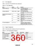
LCD Port Control Register (LPCR)
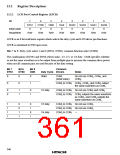
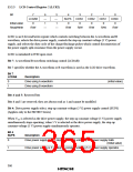
Bit
7
DTS1
0
6
DTS0
0
5
CMX
0
4
3
SGS3
0
2
SGS2
0
1
SGS1
0
0
SGS0
0
SGX
0
Initial value
Read/Write
R/W
R/W
R/W
R/W
R/W
R/W
R/W
R/W
LPCR is an 8-bit read/write register which selects the duty cycle and LCD driver pin functions.
LPCR is initialized to H'00 upon reset.
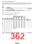
Bits 7 to 5: Duty cycle select 1 and 0 (DTS1, DTS0), common function select (CMX)
The combination of DTS1 and DTS0 selects static, 1/2, 1/3, or 1/4 duty. CMX specifies whether
or not the same waveform is to be output from multiple pins to increase the common drive power
when not all common pins are used because of the duty setting.
Bit 7
DTS1
Bit 6
DTS0
Bit 5
CMX
Common
Duty Cycle Drivers
Notes
0
0
0
Static
COM1
(initial value)
Do not use COM4, COM3, and
COM2.
0
0
1
COM4 to COM1 COM4, COM3, and COM2 output
the same waveform as COM1.
0
0
1
1
0
1
1/2 duty
COM2 to COM1 Do not use COM4 and COM3.
COM4 to COM1 COM4 outputs the same waveform
as COM3, and COM2 outputs the
same waveform as COM1.
1
1
1
1
0
0
1
1
0
1
0
1
1/3 duty
1/4 duty
COM3 to COM1 Do not use COM4.
COM4 to COM1 Do not use COM4.
COM4 to COM1
—
346

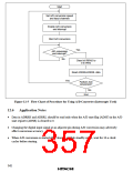
 ETC [ ETC ]