•
A or B waveform selectable by software
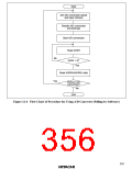
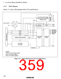
13.1.2 Block Diagram
Figure 13-1 shows a block diagram of the LCD controller/driver.
V0
V1
LCD drive power supply
(built-in step-up constant-
voltage circuit)
V2
V3
VSS
M
CL2
ø/2 to ø/256
øw
COM1
COM4
Common
driver
Common
data latch
SEG40/CL1
SEG39/CL2
SEG38/DO
SEG37/M
SEG36
LPCR
LCR
LCR2
Segment
driver
40-bit shift
register
Display timing generator
CL1
LCD RAM
(20 bytes)
SEG1
SEGn, DO
Notation:
LPCR: LCD port control register
LCR: LCD control register
LCR2: LCD control register 2
Figure 13-1 Block Diagram of LCD Controller/Driver
344

 ETC [ ETC ]