APEX 20K Programmable Logic Device Family Data Sheet
1
For DC Operating Specifications on APEX 20KE I/ O standards,
please refer to Application Note 117 (Using Selectable I/O Standards
in Altera Devices).
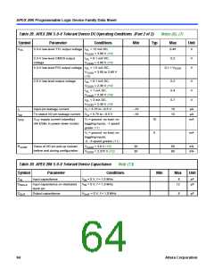
Table 34. APEX 20KE Device Capacitance
Note (13)
Conditions
Symbol
Parameter
Min
Max
Unit
CIN
Input capacitance
VIN = 0 V, f = 1.0 MHz
VIN = 0 V, f = 1.0 MHz
8
pF
pF
CINCLK
Input capacitance on dedicated
clock pin
12
COUT
Output capacitance
VOUT = 0 V, f = 1.0 MHz
8
pF
Notes to tables:
(1) See the Operating Requirements for Altera Devices Data Sheet.
(2) Minimum DC input is –0.5 V. During transitions, the inputs may undershoot to –0.5 V or overshoot to 4.6 V for
input currents less than 100 mA and periods shorter than 20 ns.
(3) Numbers in parentheses are for industrial-temperature-range devices.
(4) Maximum V rise time is 100 ms, and V must rise monotonically.
CC
CC
(5) All pins, including dedicated inputs, clock, I/ O, and JTAG pins, may be driven before V
powered.
and V
are
CCIO
CCINT
(6) Typical values are for T = 25° C, V
= 1.8 V, and V
= 1.8 V, 2.5 V or 3.3 V.
A
CCINT
CCIO
(7) These values are specified under the APEX 20KE device recommended operating conditions, shown in Table 28 on
page 63.
(8) The APEX 20KE input buffers are compatible with 1.8-V, 2.5-V and 3.3-V (LVTTL and LVCMOS) signals.
Additionally, the input buffers are 3.3-V PCI compliant. Input buffers also meet specifications for GTL+, CTT, AGP,
SSTL-2, SSTL-3, and HSTL.
(9) The I
parameter refers to high-level TTL, PCI, or CMOS output current.
OH
(10) The I parameter refers to low-level TTL, PCI, or CMOS output current. This parameter applies to open-drain pins
OL
as well as output pins.
(11) This value is specified for normal device operation. The value may vary during power-up.
(12) Pin pull-up resistance values will be lower if an external source drives the pin higher than V
(13) Capacitance is sample-tested only.
.
CCIO
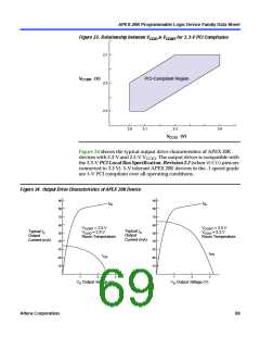
Figure 33 shows the relationship between VCCIO and VCCINT for 3.3-V PCI
compliance on APEX 20K devices.
68
Altera Corporation

 ETC [ ETC ]