APEX 20K Programmable Logic Device Family Data Sheet
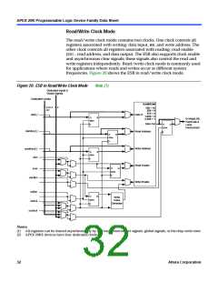
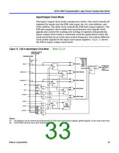
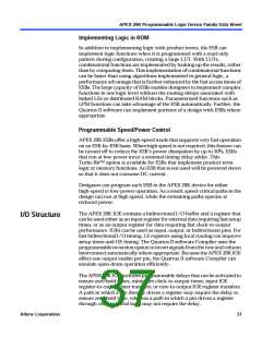
Input/Output Clock Mode
The input/ output clock mode contains two clocks. One clock controls all
registers for inputs into the ESB: data input, WE, RE, read address, and
write address. The other clock controls the ESB data output registers. The
ESB also supports clock enable and asynchronous clear signals; these
signals also control the reading and writing of registers independently.
Input/ output clock mode is commonly used for applications where the
reads and writes occur at the same system frequency, but require different
clock enable signals for the input and output registers. Figure 21 shows
the ESB in input/ output clock mode.
Figure 21. ESB in Input/Output Clock Mode
Notes (1), (2)
Dedicated Inputs &
Global Signals
Dedicated Clocks
RAM/ROM
2 or 4
(2)
4
128 × 16
256 × 8
512 × 4
1,024 × 2
2,048 × 1
data[ ]
Data In
D
Q
to MegaLAB,
FastTrack &
Local
ENA
Data Out
D
Q
ENA
Interconnect
rdaddress[ ]
Read Address
Write Address
D
Q
ENA
wraddress[ ]
rden
D
Q
ENA
Read Enable
Write Enable
D
Q
wren
ENA
outclken
inclken
inclock
D
Q
Write
Pulse
Generator
ENA
outclock
Notes:
(1) All registers can be cleared asynchronously by ESB local interconnect signals, global signals, or the chip-wide reset.
(2) APEX 20KE devices have four dedicated clocks.
Altera Corporation
33

 ETC [ ETC ]