APEX 20K Programmable Logic Device Family Data Sheet
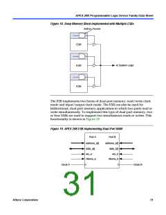
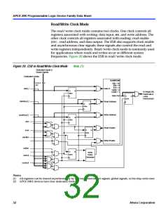
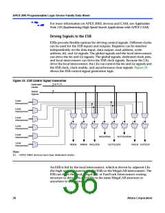
Read/Write Clock Mode
The read/ write clock mode contains two clocks. One clock controls all
registers associated with writing: data input, WE, and write address. The
other clock controls all registers associated with reading: read enable
(RE), read address, and data output. The ESB also supports clock enable
and asynchronous clear signals; these signals also control the read and
write registers independently. Read/ write clock mode is commonly used
for applications where reads and writes occur at different system
frequencies. Figure 20 shows the ESB in read/ write clock mode.
Figure 20. ESB in Read/Write Clock Mode
Note (1)
Dedicated Inputs &
Global Signals
Dedicated Clocks
RAM/ROM
2 or 4
(2)
4
128 × 16
256 × 8
512 × 4
1,024 × 2
2,048 × 1
data[ ]
Data In
D
Q
to MegaLAB,
FastTrack &
Local
ENA
Data Out
D
Q
ENA
Interconnect
rdaddress[ ]
Read Address
Write Address
D
Q
ENA
wraddress[ ]
rden
D
Q
ENA
Read Enable
Write Enable
D
Q
wren
ENA
outclken
inclken
inclock
D
Q
Write
Pulse
Generator
ENA
outclock
Notes:
(1) All registers can be cleared asynchronously by ESB local interconnect signals, global signals, or the chip-wide reset.
(2) APEX 20KE devices have four dedicated clocks.
32
Altera Corporation

 ETC [ ETC ]