Si3035
Table 6. Absolute Maximum Ratings
Parameter
Symbol
VD, VA
IIN
Value
–0.5 to 6.0
±10
Unit
V
DC Supply Voltage
Input Current, Si3021 Digital Input Pins
Digital Input Voltage
mA
V
VIND
TA
–0.3 to (VD + 0.3)
–40 to 100
–65 to 150
Operating Temperature Range
Storage Temperature Range
°C
°C
TSTG
Note: Permanent device damage may occur if the above Absolute Maximum Ratings are exceeded. Functional operation
should be restricted to the conditions as specified in the operational sections of this data sheet. Exposure to absolute
maximum rating conditions for extended periods may affect device reliability.
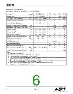
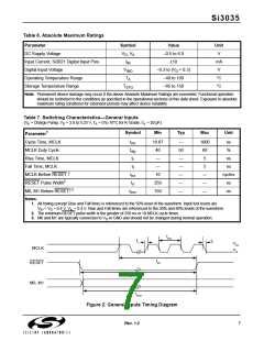
Table 7. Switching Characteristics—General Inputs
(VA = Charge Pump, VD = 3.0 to 5.25 V, TA = 0 to 70°C for K-Grade, CL = 20 pF)
Parameter1
Symbol
Min
Typ
Max
Unit
Cycle Time, MCLK
MCLK Duty Cycle
Rise Time, MCLK
Fall Time, MCLK
MCLK Before RESET ↑
RESET Pulse Width2
M0, M1 Before RESET↑3
Notes:
tmc
tdty
tr
16.67
40
—
50
—
—
—
—
—
1000
60
5
ns
%
—
ns
tf
—
5
ns
tmr
trl
10
—
—
—
cycles
ns
250
150
tmxr
ns
1. All timing (except Rise and Fall time) is referenced to the 50% level of the waveform. Input test levels are
VIH = VD – 0.4 V, VIL = 0.4 V. Rise and Fall times are referenced to the 20% and 80% levels of the waveform.
2. The minimum RESET pulse width is the greater of 250 ns or 10 MCLK cycle times.
3. M0 and M1 are typically connected to VD or GND and should not be changed during normal operation.
tmc
tr
tf
VIH
VIL
MCLK
tmr
RESET
trl
M0, M1
tmxr
Figure 2. General Inputs Timing Diagram
Rev. 1.2
7

 ETC [ ETC ]