Si3035
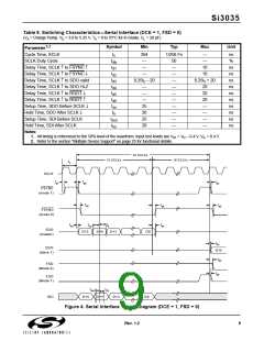
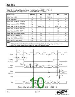
Table 10. Switching Characteristics—Serial Interface (DCE = 1, FSD = 1)
(VA = Charge Pump, VD = 3.0 to 5.25 V, TA = 0 to 70°C for K-Grade, CL = 20 pF)
Parameter1,2
Symbol
Min
Typ
Max
Unit
Cycle Time, SCLK
tc
tdty
td1
td2
td3
td4
td5
tsu
th
354
1/256 Fs
—
ns
%
SCLK Duty Cycle
—
50
—
—
—
—
—
—
—
—
—
—
Delay Time, SCLK ↑ to FSYNC ↑
Delay Time, SCLK ↑ to FSYNC ↓
Delay Time, SCLK ↑ to SDO valid
Delay Time, SCLK ↑ to SDO Hi-Z
Delay Time, SCLK ↑ to RGDT ↓
Setup Time, SDO Before SCLK ↓
Hold Time, SDO After SCLK ↓
Setup Time, SDI Before SCLK
Hold Time, SDI After SCLK
Notes:
—
10
ns
ns
ns
ns
ns
ns
ns
ns
ns
—
10
0.25tc – 20
0.25tc + 20
—
—
25
20
25
20
20
20
—
—
—
—
tsu2
th2
1. All timing is referenced to the 50% level of the waveform. Input test levels are VIH = VD – 0.4 V, VIL = 0.4 V.
2. Refer to the section "Multiple Device Support" on page 25 for functional details.
tc
SCLK
td1
td2
FSYNC
(mode 1)
td3
tsu
th
td4
SDO
(master)
D15
D14
D13
D0
td3
D15
td5
SDO
(slave 1)
FSD
SDI
tsu2
th2
D14
D15
D1
D0
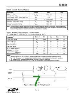
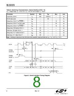
Figure 5. Serial Interface Timing Diagram (DCE = 1, FSD = 1)
10
Rev. 1.2

 ETC [ ETC ]