Si3035
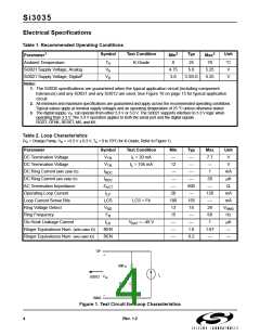
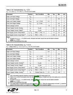
Table 3. DC Characteristics, V = +5 V
D
(VA = +5 V ±5%, VD = +5 V ±5%, TA = 0 to 70°C for K-Grade)
Parameter
Symbol
VIH
Test Condition
Min
3.5
—
Typ
—
Max
Unit
V
High Level Input Voltage
Low Level Input Voltage
High Level Output Voltage
Low Level Output Voltage
Input Leakage Current
—
0.8
—
VIL
—
V
VOH
VOL
IL
IO = –2 mA
IO = 2 mA
3.5
—
—
V
—
0.4
10
1
V
–10
—
—
µA
mA
mA
mA
mA
Power Supply Current, Analog
Power Supply Current, Digital1
Total Supply Current, Sleep Mode1
Total Supply Current, Deep Sleep1,2
Notes:
IA
VA pin
0.3
14
ID
VD pin
—
18
2.5
0.5
IA + ID
IA + ID
PDN = 1, PDL = 0
PDN = 1, PDL = 1
—
1.3
0.04
—
1. All inputs at 0.4 or VD – 0.4 (CMOS levels). All inputs held static except clock and all outputs unloaded
(Static IOUT = 0 mA).
2. RGDT is not functional in this state.
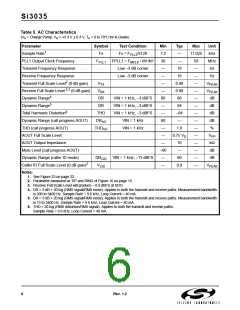
Table 4. DC Characteristics, V = +3.3 V
D
(VA = Charge Pump, VD = +3.3 V ± 0.3 V, TA = 0 to 70°C for K-Grade)
Parameter
Symbol
VIH
Test Condition
Min
2.0
—
Typ
—
Max
—
Unit
V
High Level Input Voltage
Low Level Input Voltage
High Level Output Voltage
Low Level Output Voltage
Input Leakage Current
VIL
—
0.8
—
V
VOH
VOL
IL
IO = –2 mA
IO = 2 mA
2.4
—
—
V
—
0.35
10
V
–10
—
—
µA
mA
mA
mA
Power Supply Current, Analog1,2
Power Supply Current, Digital3
Total Supply Current, Sleep Mode3
Total Supply Current, Deep Sleep3,4
Power Supply Voltage, Analog1,5
Notes:
IA
VA pin
0.3
9
1
ID
VD pin
—
12
IA + ID
IA + ID
VA
PDN = 1, PDL = 0
PDN = 1, PDL = 1
Charge Pump On
—
1.2
0.04
4.6
2.5
0.5
5.00
—
4.3
V
1. Only a decoupling capacitor should be connected to VA when the charge pump is on.
2. There is no IA current consumption when the internal charge pump is enabled and only a decoupling cap is connected
to the VA pin.
3. All inputs at 0.4 or VD – 0.4 (CMOS levels). All inputs held static except clock and all outputs unloaded
(Static IOUT = 0 mA).
4. RGDT is not functional in this state.
5. The charge pump is recommended to be used only when VD < 4.5 V. When the charge pump is not used, VA should be
applied to the device before VD is applied on power up if driven from separate supplies.
Rev. 1.2
5

 ETC [ ETC ]