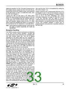
Si3035
digital test waveform on SDI. This data is passed across chip must be reset. This is accomplished by setting the
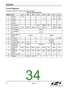
the isolation barrier, looped from the TX to the RX pin, PDL bit for at least 1 ms.
passed back across the isolation barrier, and presented
to the data pump on SDO. To enable this mode, clear
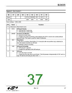
bit (Register 12, bit 7). The CLE bit indicates a time-out
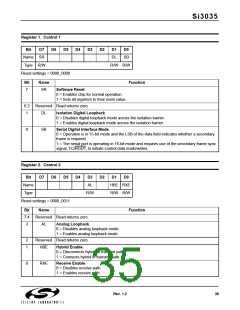
the HBE bit of Register 2.
Another useful bit is the communication link error (CLE)
error for the ISOcap link following a change to either
Clearing the HBE bit will cause a DC offset which PLL1 or PLL2. For more information, see “Clock
affects the signal swing of the transmit signal. In this test Generation Subsystem” on page 20. When the CLE bit
mode, it is recommended that the transmit signal be is set, the DSP-side chip has failed to receive
12 dB lower than normal transmit levels. This lower verification from the line side that the clock change has
level will eliminate clipping caused by the DC offset been accepted in an expected period of time (less than
which results from disabling the hybrid. It is assumed in 10 ms). This condition indicates a severe error in
this test that the line AC impedance is nominally 600 Ω. programming the clock generator or possibly a defective
line-side chip.
Note: All test modes are mutually exclusive. If more than one
test mode is enabled concurrently, the results are
unpredictable.
Exception Handling
The Si3035 provides several mechanisms to determine
if an error occurs during operation. Through the
secondary frames of the serial link, the controlling DSP
can read several status bits. The bit of highest
importance is the frame detect bit (FDT, Register 12,
bit 6). This bit indicates that the DSP-side (Si3021) and
line-side (Si3012) devices are communicating. During
normal operation, the FDT bit can be checked before
reading any bits that indicate information about the line
side. If FDT is not set, the following bits related to the
line-side are invalid: RDT, LCS, CBID, and REVB. The
RGDT operation will also be non-functional.
Following power-up and reset, the FDT bit is not set
because the PDL bit (Register 6, bit 4) defaults to 1. In
this state, the ISOcap link is not operating and no
information about the line-side can be determined. The
user must program the clock generator to a valid
configuration for the system and clear the PDL bit to
activate the ISOcap link. While the Si3021 and Si3012
are establishing communication, the Si3035 will not
generate FSYNC signals. Establishing communication
will take less than 10 ms. Therefore, if the controlling
DSP serial interface is interrupt driven, based on the
FSYNC signal, the controlling DSP does not require a
special delay loop to wait for this event to complete.
The FDT bit can also indicate if the line-side executes
an off-hook request successfully. If the line-side is not
connected to a phone line (i.e., the user fails to connect
a phone line to the modem), the FDT bit remains
cleared. The controlling DSP must allow sufficient time
for the line-side to execute the off-hook request. The
maximum time for FDT to be valid following an off-hook
request is 10 ms. At this time, the LCS bits indicate the
amount of loop current flowing. For more information,
see “Loop Current Monitor” on page 25. If the FDT bit
fails to be set following an off-hook request, the line-side
Rev. 1.2
33

 ETC [ ETC ]