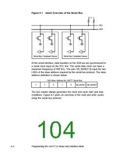
Figure A.1 Quick Overview of the Serial Bus
5 V
SCL
SDA
Serial Bus Compliant Device
Serial Bus Compliant Device
At the serial interface, data transfers on the SDA pin are synchronized to
a serial clock input on the SCL line. The serial data clock can have a
maximum frequency of 400 kHz. The pins SB_BASE[1:0] input the two
LSB’s of the slave address required by the serial bus protocol. The slave
address definition is shown below:
7-Bit Slave Address for L64777 Serial Bus
1
1
0
1
0
SB_BASE1 SB_BASE0
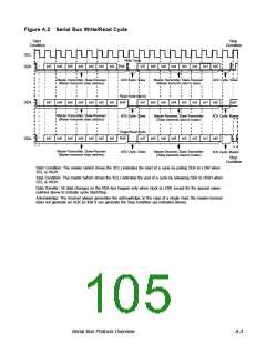
The bus master always generates the clock and cycle start and stop
conditions. Figure A.2 gives an overview of the read and write cycles
using the serial bus protocol.
A-2
Programming the L64777 in Serial Host Interface Mode

 ETC [ ETC ]