Register Description
3.3.30
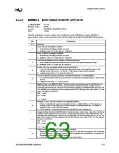
ERRSTS—Error Status Register (Device 0)
Address Offset:
Default Value:
Access:
91–92h
0000h
Read Only, Read/Write Clear
16 bits
Size:
This 16-bit register is used to report error conditions via the SERR# mechanism. SERR# is
generated on a zero to one transition of any of these flags (if enabled by the ERRCMD register).
Bit
Description
15:13
Reserved.
Read thermal Throttling Condition.
12
11
10
1 = Read thermal throttling condition occurred.
0 = Software writes “1” to clear this bit. Default=0
Write Thermal Throttling Condition.
1 = Write thermal throttling condition occurred.
0 = Software writes “1” to clear this bit. Default=0
AGP non-snoopable access outside of Graphics Aperture.
1 = AGP access occurred to the address that is outside of the graphics aperture range.
0 = Software writes “1” to clear this bit. Default=0
Invalid AGP non-snoopable DRAM read access (R/WC).
1 = AGP non-snoopable READ access was attempted outside of the graphics aperture and
outside of main memory (i.e,. in 640 KB – 1 MB range or above top of memory).
9
8
0 = Software must write a “1” to clear this status bit.
Access to Invalid Graphics Aperture Translation Table Entry (AIGATT) (R\WC).
1 = An invalid translation table entry was returned in response to a graphics aperture read or write
access.
0 = Software must write a “1” to clear this bit.
Multi-bit First Error (MBFRE) (RO). This field contains the encoded value of the DRAM row in
which the first multi-bit error occurred. A simple binary encoding is used to indicate the row
containing the multi-bit error. When an error is detected, this field is updated and the MEF bit is set.
This field will then be locked (no further updates) until the MEF flag has been reset. If MEF is 0, the
value in this field is undefined.
7:5
000 = Row 0
001 = Row 1
...
111 = Row 7
Multiple-bit ECC (uncorrectable) Error Flag (MEF) (R/WC).
1 = Memory data transfer had an uncorrectable error(i.e., multiple-bit error). When enabled, a
multiple bit error is reported by the DRAM controller and propagated to the SERR# pin, if
enabled by bit 1 in the ERRCMD register.
4
0 = BIOS writes a 1 to clear this bit and unlock the MBFRE field. (Default = 0).
Single-bit First Row Error (SBFRE) (RO). This field contains the encoded value of the DRAM row
in which the first single-bit error occurred. A simple binary encoding is used to indicate the row
containing the single-bit error. When an error is detected, this field is updated and SEF is set. This
field is then locked (no further updates) until the SEF flag has been reset. If SEF is 0, the value in
this field is undefined.
3:1
000 = Row 0
001 = Row 1
...
111 = Row 7
Single-bit (correctable) ECC Error Flag (SEF) (R/WC).
1 = Memory data transfer had a single-bit correctable error and the corrected data was sent for the
access. When ECC is enabled, a single bit error is reported and propagated to the SERR# pin,
if enabled by bit 0 in the ERRCMD register.
0
0 = BIOS writes a 1 to clear this bit and unlock the SBFRE field.
82443BX Host Bridge Datasheet
3-37

 ETC [ ETC ]