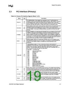
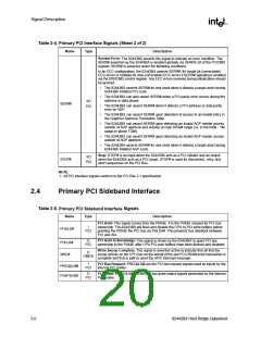
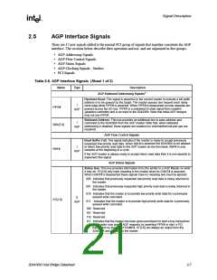
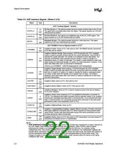
Signal Description
Table 2-3.
Signals (Sheet 2 of 2)
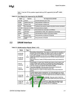
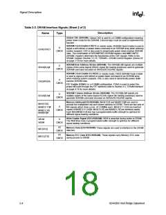
DRAM Interface
Description
Name
Type
Global CKE (SDRAM): Global CKE is used in a 4 DIMM configuration requiring
power down mode for the SDRAM. External logic must be used to implement this
function.
SDRAM Clock Enable (CKE1): In mobile mode, SDRAM Clock Enable is used to
signal a self-refresh or power-down command to an SDRAM array when entering
system suspend. CKE is also used to dynamically power down inactive SDRAM
rows. The combination of SDRAMPWR (SDRAM register) and MMCONFIG
(DRAMC register) determine the functioning of the CKE signals. Refer to the
DRAMC register (Section 3.3.15, “DRAMC—DRAM Control Register (Device 0)”
on page 3-19) for more details.
O
GCKE/CKE1
CMOS
SDRAM Row Address Strobe (SDRAM): The SRAS[B,A]# signals are multiple
copies of the same logical SRASx signal (for loading purposes) used to generate
SDRAM command encoded on SRASx/SCASx/WE signals.
O
SRAS[B,A]#
CKE0/FENA
SCAS[B,A]#
CMOS
SDRAM Clock Enable 0 (CKE0). In mobile mode, CKE0 SDRAM Clock Enable
is used to signal a self-refresh or power-down command to an SDRAM array
when entering system suspend. CKE is also used to dynamically power down
inactive SDRAM rows.
O
CMOS
FET Enable (FENA): In a 4 DIMM configuration. FENA is used to select the
proper MD path through the FET switches (refer to Section 4.3, “DRAM Interface”
on page 4-14 for more details).
SDRAM Column Address Strobe (SDRAM): The SCAS[B,A]# signals are
multiple copies of the same logical SCASx signal (for loading purposes) used to
generate SDRAM command encoded on SRASx/SCASx/WE signals.
O
CMOS
Memory Address(EDO/SDRAM): MAA[13:0] and MAB[13:0]# are used to
provide the multiplexed row and column address to DRAM. There are two sets of
MA signals which drive a max. of 2 DIMMs each. MAA[12:11,9:0] are inverted
copies of MAB[12:11,9:0]#. MAA[13,10] and MAB[13,10] are identical copies.
Each MAA/MAB[13:0] line has a programmable buffer strength to optimize for
different signal loading conditions.
MAA[13:0]
O
MAB[12:11]#
CMOS
MAB[13,10]
MAB[9:0]#
Write Enable Signal (EDO/SDRAM): WE# is asserted during writes to DRAM.
The WE# lines have a programmable buffer strength to optimize for different
signal loading conditions.
WEA#
WEB#
O
CMOS
I/O
Memory Data (EDO/SDRAM): These signals are used to interface to the DRAM
data bus.
MD [63:0]
CMOS
I/O
Memory ECC Data (EDO/SDRAM): These signals carry Memory ECC data
during access to DRAM.
MECC[7:0]
CMOS
2-4
82443BX Host Bridge Datasheet

 ETC [ ETC ]