Signal Description
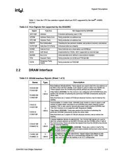
Table 2-2 lists the CPU bus interface signals which are NOT supported by the Intel® 440BX
AGPset.
Table 2-2. Host Signals Not supported by the 82443BX
Signal
Function
Address
Not Supported By 82443BX
Extended addressing (over 4 GB)
A[35:32]#
AERR#
AP[1:0]#
BINIT#
DEP[7:0]#
IERR#
Address Parity Error
Address Parity
Bus Initialization
Data Bus ECC/Parity
Internal Error
Parity protection on address bus
Parity protection on address bus
Checking for bus protocol violation and protocol recovery mechanism
Enhanced data bus integrity
Direct internal error observation via IERR# pin
Implemented by PIIX4E, BIST supported by external logic.
Unrecoverable error without a bus protocol violation
Parity protection on ADS# and PREQ[4:0]#
INIT#
Soft Reset
BERR#
RP#
Bus Error
Request Parity
Response Parity
Signal
RSP#
Parity protection on RS[2:0]#
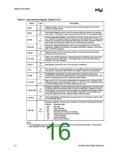
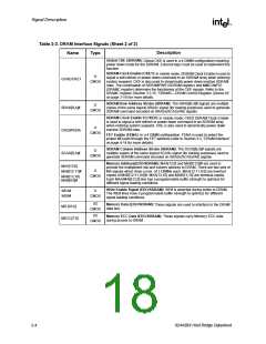
2.2
DRAM Interface
Table 2-3.
Signals (Sheet 1 of 2)
DRAM Interface
Description
Name
Type
Row Address Strobe (EDO): These signals are used to latch the row address on
the MAxx lines into the DRAMs. Each signal is used to select one DRAM row.
These signals drive the DRAM array directly without any external buffers.
RASA[5:0]#
/CSA[5:0]#
O
Chip Select (SDRAM): For the memory row configured with SDRAM these pins
perform the function of selecting the particular SDRAM components during the
active state.
CMOS
RASB[5:0]#
/CSB[5:0]#
Note that there are 2 copies of RAS# per physical memory row to improve the
loading.
Clock Enable: In mobile mode, SDRAM Clock Enable is used to signal a self-
refresh or power-down command to an SDRAM array when entering system
suspend. CKE is also used to dynamically power down inactive SDRAM rows.
This CKE function is not supported with Registered DIMMs.
CKE[3:2]
/CSA[7:6]#
O
Chip Select (SDRAM): These pins perform the function of selecting the
particular SDRAM components during the active state.
CMOS
CKE[5:4]
/CSB[7:6]#
Note that there are 2 copies of CS# per physical memory row to reduce the
loading.
Column Address Strobe A-side (EDO): The CASA[7:0]# signals are used to
latch the column address on the MA[13:0] lines into the DRAMs of the A half of
the memory array. These are active low signals that drive the DRAM array directly
without external buffering.
CASA[7:0]#
/DQMA[7:0]
O
CMOS
Input/Output Data Mask A-side (SDRAM): These pins control A half of the
memory array and act as synchronized output enables during read cycles and as
a byte enables during write cycles.
Column Address Strobe B-side (EDO) / Input/Output Data Mask B-side
(SDRAM): The same function as a corresponding signals for A side. These
signals are used to reduce the loading in an ECC configuration
CASB[1,5]#
/DQMB[1,5]
O
CMOS
82443BX Host Bridge Datasheet
2-3

 ETC [ ETC ]