AN-32
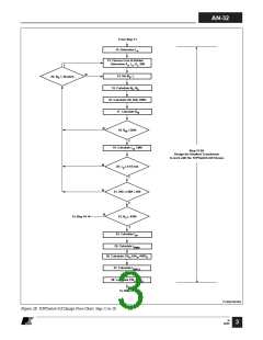
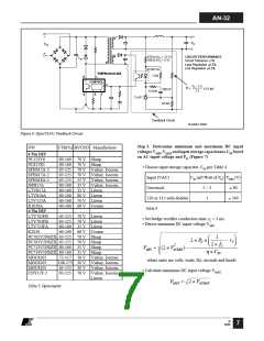
1. System Requirements
VACMIN, VACMAX, fL, VO, PO, η, Z
Step 1-2
Determine System Level Requirements
and Choose Feedback Circuit
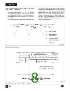
2. Choose Feedback Circuit & VB
3. Determine CIN, VMIN, VMAX
4. Determine VOR, VCLO
5. Set KP
6. Determine DMAX
Step 3-11
Choose The Smallest TOPSwitch-GX
For The Required Power
7. Calculate Primary Peak Current IP
8. Calculate Primary RMS Current IRMS
9. Choose TOPSwitch-GX & fS Using AN-29
10. Set ILIMIT Reduction Factor KI
Calculate ILIMIT (min) & ILIMIT (max)
From Step 23
N
11. IP ≤ ILIMIT (min)
Y
To Step 12
PI-3039-080502
Figure 2A. TOPSwitch-GX Design Flow Chart. Step 1 to 11.
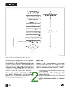
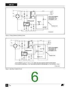
specificissuessuchasconstantcurrent,constantpoweroutputs,
etc. are beyond the scope of this application note. However,
suchrequirementsmaybesatisfiedbyaddingadditionalcircuitry
to the basic converter configuration. The only part of the circuit
configuration that may change from application to application
isthefeedbackcircuitry.Dependingonthepowersupplyoutput
specifications, one of the four feedback circuits, shown in
Figures 3, 4, 5 and 6, will be chosen for the application.
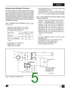
Design Flow
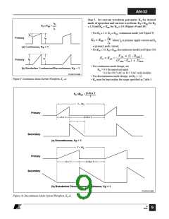
Figures 2A, 2B and 2C present a design flow chart showing the
complete design procedure in 37 steps. With the basic circuit
configuration shown in Figure 1 as its foundation, the logic
behind this design approach can be summarized as follows:
1. Determine system requirements and decide on feedback
circuit accordingly.
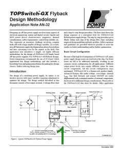
The basic circuit configuration used in TOPSwitch-GX flyback
power supplies is shown in Figure 1, which also serves as the
reference circuit for component identifications used in the
description throughout this application note.
2. Choose the smallest TOPSwitch-GX capable of the
required output power.
3. Design the smallest transformer for the TOPSwitch-GX
chosen.
4. Select all other components in Figure 1 to complete the
design.
B
12/02
2

 ETC [ ETC ]