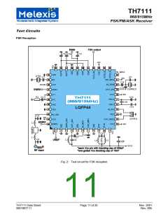
TH7111
868/915MHz
FSK/FM/ASK Receiver
Technical Data
Mode Configurations
ENRX
ENRO
Mode
Description
0
0
1
1
0
1
0
1
SBY
RO only
ON
standby mode
only reference oscillator active
entire chip active
ON
entire chip active
Note: ENRX and ENRO are pulled down internally
Second Mixer Input
IN_MIX2V
External LO2
Ext. pull-down res. (15 kΩ)
SW_MIX2
Mode
0
0
1
double conversion with external LO2
single conversion
double conversion with internal LO2
N/C
LNA Gain Control
VGAIN_LNA
< 0.8 V
> 1.4 V
Mode
Description
HIGH GAIN
LOW GAIN
LNA set to high gain by voltage at GAIN_LNA
LNA set to low gain by voltage at GAIN_LNA
Note: hysteresis between gain modes to ensure stability
Absolute Maximum Ratings
Parameter
Supply voltage
Input voltage
Input RF level
Storage temperature
Electrostatic discharge
Symbol
Vcc
VIN
Pimax
TSTG
ESD
Condition / Note
Min
Max
Unit
0
- 0.3
7.0
VCC+0.3
10
V
V
dBm
°C
no damage
-40
+125
human body model,
MIL STD 833D
method 3015.7, all pins
except OUT_IFA
pin OUT_IFA
-500
-500
+500
+250
V
V
Normal Operating Conditions
Parameter
Symbol
Condition
Min
Max
Unit
Supply voltage for double conv.
Supply voltage for single conv.
Operating temperature
Input frequency
Frequency deviation
FSK data rate
Vcc, DC
Vcc, SC
Ta
fi
∆f
RFSK
fm
RASK
2.5
3.3
-40
800
±5
5.5
5.5
+85
930
±120
40
V
V
ºC
MHz
kHz
kbit/s
kHz
kbit/s
at FM or FSK
NRZ
FM bandwidth
ASK data rate
15
80
NRZ
TH7111 Data Sheet
3901007111
Page 9 of 20
Nov. 2001
Rev. 005

 ETC [ ETC ]