TH7111
868/915MHz
FSK/FM/ASK Receiver
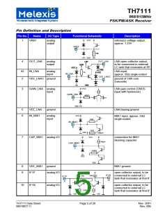
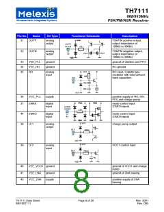
Pin No.
Name
I/O Type
Functional Schematic
Description
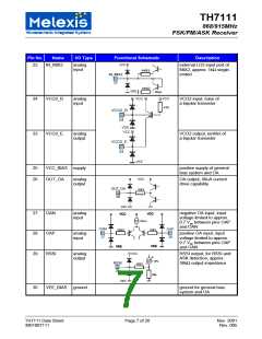
22
IN_MIX2
analog
input
external LO2 input port of
MIX2, approx. 1kΩ single-
ended
840Ω
IN_MIX2
22
840Ω
20µA
VCC
VCC
47k
24
23
VCO2_B
VCO2_E
analog
input
VCO2 input, base of
a bipolar transistor
VCO2_B
24
VEE
VCC
analog
output
VCO2 output, emitter of
a bipolar transistor
VCO2_E
23
VEE
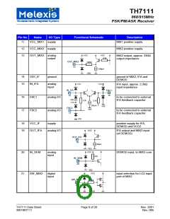
25
26
VCC_BIAS supply
positive supply of general
bias system and OA
OUT_OA
analog
output
OA output, 40uA current
drive capability
OUT_OA
26
50
Ω
27
28
29
OAN
OAP
RSSI
analog
input
negative OA input, input
voltage limited to approx.
0.7 Vpp between pins OAP
and OAN
20µA
OAN
27
OAP
28
50
Ω
50Ω
analog
input
positive OA input, input
voltage limited to approx.
0.7 Vpp between pins OAP
and OAN
analog
output
RSSI output, for RSSI and
ASK detection, approx.
36kΩ output impedance
I (Pi)
36k
RSSI
29
50Ω
30
VEE_BIAS ground
ground for general bias
system and OA
TH7111 Data Sheet
3901007111
Page 7 of 20
Nov. 2001
Rev. 005

 ETC [ ETC ]