TH7111
868/915MHz
FSK/FM/ASK Receiver
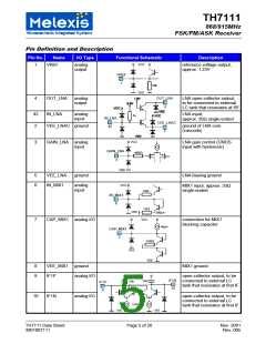
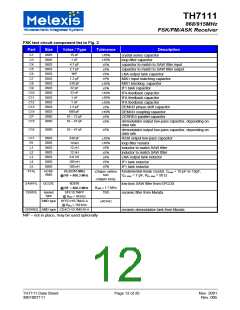
Pin No.
Name
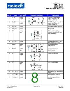
OUTP
I/O Type
Functional Schematic
Description
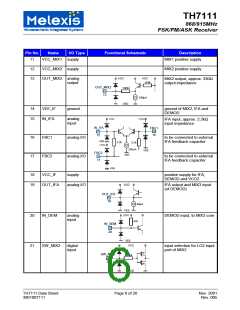
31
analog
output
FSK/FM positive output,
output impedance of
100kΩ to 300kΩ
OUTP
OUTN
50
Ω
32
OUTN
analog
output
FSK/FM negative output,
output impedance of
100kΩ to 300kΩ
31
32
20µA
20µA
33
34
35
VEE_PLL
VEE_RO
RO
ground
ground
ground of dividers and PFD
RO ground
analog
input
RO input, Colpitts type
oscillator with internal feed-
back capacitors
50k
30p
RO
35
30p
36
37
VCC_PLL
ENRX
supply
positive supply of RO, DIV,
PFD and charge pump
digital
input
mode control input
(CMOS input)
ENRX
ENRO
1.5k
44
38
ENRO
LF1
digital
input
mode control input
(CMOS input)
37
44
analog
output
charge pump output
VCO1 control input
LF1
38
200
Ω
39
40
LF2
analog
input
LF2
39
400
Ω
4p
VEE_VCO1 ground
ground of VCO1 and charge
pump
41
43
VEE_LNA
VCC_LNA
ground
supply
ground of LNA biasing
positive supply of LNA
biasing
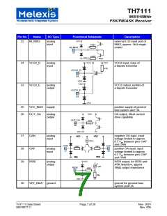
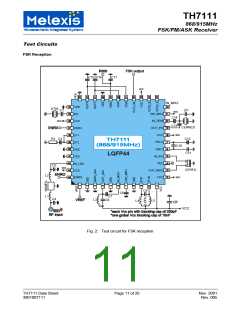
TH7111 Data Sheet
3901007111
Page 8 of 20
Nov. 2001
Rev. 005

 ETC [ ETC ]