TH7111
868/915MHz
FSK/FM/ASK Receiver
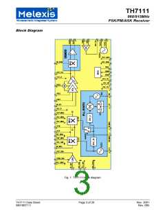
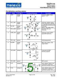
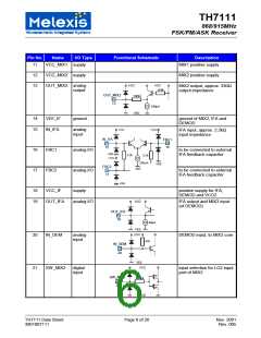
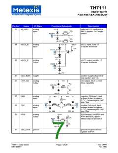
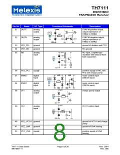
Pin Definition and Description
Pin No.
Name
VREF
I/O Type
Functional Schematic
Description
1
analog
output
reference voltage output,
approx. 1.23V
VREF
1
60k
OUT_LNA
4
OUT_LNA
IN_LNA
analog
output
LNA open-collector output,
to be connected to external
LC tank that resonates at RF
4
42
2
analog
input
LNA input,
approx. 26Ω single-ended
5k
IN_LNA
42
VEE_LNAC
2
VEE_LNAC ground
ground of LNA core
(cascode)
3
GAIN_LNA analog
input
LNA gain control (CMOS
input with hysteresis)
GAIN_LNA
3
400
Ω
5
6
VEE_LNA
IN_MIX1
ground
LNA biasing ground
analog
input
MIX1 input, approx. 33Ω
single-ended
13Ω
IN_MIX1
6
13Ω
500µA
40µA
7
CAP_MIX1 analog I/O
connection for MIX1
blocking capacitor
CAP_MIX1
7
330
Ω
8
9
VEE_MIX1 ground
MIX1 ground
VCC
IF1P
analog I/O
open-collector output, to be
connected to external LC
tank that resonates at first IF
IF1N
10
20p
20p
IF1P
9
10
IF1N
analog I/O
open-collector output, to be
connected to external LC
tank that resonates at first IF
2x500µA
VEE
VEE
TH7111 Data Sheet
3901007111
Page 5 of 20
Nov. 2001
Rev. 005

 ETC [ ETC ]