NT5DS32M4AT
NT5DS16M8AT
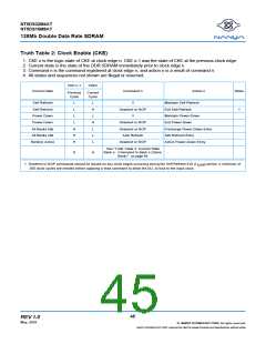
128Mb Double Data Rate SDRAM
Truth Table 2: Clock Enable (CKE)
1. CKE n is the logic state of CKE at clock edge n: CKE n-1 was the state of CKE at the previous clock edge.
2. Current state is the state of the DDR SDRAM immediately prior to clock edge n.
3. Command n is the command registered at clock edge n, and action n is a result of command n.
4. All states and sequences not shown are illegal or reserved.
CKE n-1
CKEn
Current State
Command n
Action n
Notes
Previous
Cycle
Current
Cycle
Self Refresh
Self Refresh
Power Down
Power Down
All Banks Idle
All Banks Idle
Bank(s) Active
L
L
L
H
L
X
Maintain Self-Refresh
Deselect or NOP
X
Exit Self-Refresh
1
L
Maintain Power-Down
Exit Power-Down
L
H
L
Deselect or NOP
Deselect or NOP
Auto Refresh
Deselect or NOP
H
H
H
Precharge Power-Down Entry
Self Refresh Entry
L
L
Active Power-Down Entry
See “Truth Table 3: Current State
Bank n - Command to Bank n (Same
Bank)” on page 46
H
H
1. Deselect or NOP commands should be issued on any clock edges occurring during the Self Refresh Exit (t
200 clock cycles are needed before applying a read command to allow the DLL to lock to the input clock.
) period. A minimum of
XSNR
45
REV 1.0
May, 2001
©
NANYA TECHNOLOGY CORP. All rights reserved.
NANYA TECHNOLOGY CORP. reserves the right to change Products and Specifications without notice.

 ETC [ ETC ]