NT5DS32M4AT
NT5DS16M8AT
128Mb Double Data Rate SDRAM
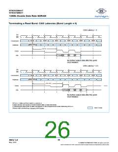
Writes
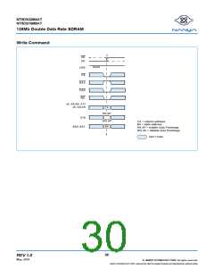
Write bursts are initiated with a Write command, as shown in timing figure Write Command on page 30.
The starting column and bank addresses are provided with the Write command, and Auto Precharge is either enabled or dis-
abled for that access. If Auto Precharge is enabled, the row being accessed is precharged at the completion of the burst. For
the generic Write commands used in the following illustrations, Auto Precharge is disabled.
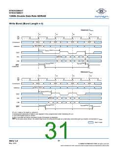
During Write bursts, the first valid data-in element is registered on the first rising edge of DQS following the write command, and
subsequent data elements are registered on successive edges of DQS. The Low state on DQS between the Write command
and the first rising edge is known as the write preamble; the Low state on DQS following the last data-in element is known as
the write postamble. The time between the Write command and the first corresponding rising edge of DQS (tDQSS) is specified
with a relatively wide range (from 75% to 125% of one clock cycle), so most of the Write diagrams that follow are drawn for the
two extreme cases (i.e. tDQSS(min) and tDQSS(max)). Timing figure Write Burst (Burst Length = 4) on page 31 shows the two
extremes of tDQSS for a burst of four. Upon completion of a burst, assuming no other commands have been initiated, the DQs
and DQS enters High-Z and any additional input data is ignored.
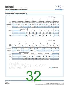
Data for any Write burst may be concatenated with or truncated with a subsequent Write command. In either case, a continuous
flow of input data can be maintained. The new Write command can be issued on any positive edge of clock following the previ-
ous Write command. The first data element from the new burst is applied after either the last element of a completed burst or
the last desired data element of a longer burst which is being truncated. The new Write command should be issued x cycles
after the first Write command, where x equals the number of desired data element pairs (pairs are required by the 2n prefetch
architecture). Timing figure Write to Write (Burst Length = 4) on page 32 shows concatenated bursts of 4. An example of non-
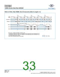
consecutive Writes is shown in timing figure Write to Write: Max DQSS, Non-Consecutive (Burst Length = 4) on page 33. Full-
speed random write accesses within a page or pages can be performed as shown in timing figure Random Write Cycles (Burst
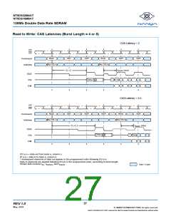
Length = 2, 4 or 8) on page 34. Data for any Write burst may be followed by a subsequent Read command. To follow a Write
without truncating the write burst, tWTR (Write to Read) should be met as shown in timing figure Write to Read: Non-Interrupting
(CAS Latency = 2; Burst Length = 4) on page 35.
Data for any Write burst may be truncated by a subsequent (interrupting) Read command. This is illustrated in timing figures
“Write to Read: Interrupting (CAS Latency =2; Burst Length = 8)”, “Write to Read: Minimum DQSS, Odd Number of Data (3 bit
Write), Interrupting (CAS Latency = 2; Burst Length = 8)”, and “Write to Read: Nominal DQSS, Interrupting (CAS Latency = 2;
Burst Length = 8)”. Note that only the data-in pairs that are registered prior to the tWTR period are written to the internal array,
and any subsequent data-in must be masked with DM, as shown in the diagrams noted previously.
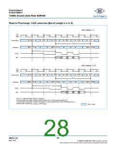
Data for any Write burst may be followed by a subsequent Precharge command. To follow a Write without truncating the write
burst, tWR should be met as shown in timing figure Write to Precharge: Non-Interrupting (Burst Length = 4) on page 39.
Data for any Write burst may be truncated by a subsequent Precharge command, as shown in timing figures Write to Pre-
charge: Interrupting (Burst Length = 4 or 8) on page 40 to Write to Precharge: Nominal DQSS (2 bit Write), Interrupting (Burst
Length = 4 or 8) on page 42. Note that only the data-in pairs that are registered prior to the tWR period are written to the internal
array, and any subsequent data in should be masked with DM. Following the Precharge command, a subsequent command to
the same bank cannot be issued until tRP is met.
In the case of a Write burst being executed to completion, a Precharge command issued at the optimum time (as described
above) provides the same operation that would result from the same burst with Auto Precharge. The disadvantage of the Pre-
charge command is that it requires that the command and address busses be available at the appropriate time to issue the com-
mand. The advantage of the Precharge command is that it can be used to truncate bursts.
29
REV 1.0
May, 2001
©
NANYA TECHNOLOGY CORP. All rights reserved.
NANYA TECHNOLOGY CORP. reserves the right to change Products and Specifications without notice.

 ETC [ ETC ]