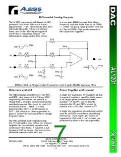
Differen t ial An alog Ou t p u t s
Th e AL1201 ou tpu ts are self-biased to MID
is a two-pole 48kHz lowpass filter wh ose
frequ en cy response is flat from dc to 20kHz
+/ -.03dB. Its grou p delay deviation from flat
is 1.3µs at 20kHz. High qu ality ceram ic or
film capacitors su ggested.
poten tial. Maxim u m differential ou tpu t
sign al level is +/ -4V. Th e ou tpu ts h ave been
in tern ally filtered to redu ce ou t-of-ban d
n oise, an d fu rther filtering is su ggested
where th is is considered critical. Th e
differen tial-to-sin gle-en ded filter shown
8.2k
4Vpp
390p
MID
10µ
10µ
8.2k
1.8k
1.8k
IN-
Ou t
1000p
8.2k
8Vpp
GND
IN+
390p
GND
8.2k
4Vpp
GND
MID
Differen tial to Sin gle-en ded Con verter an d 2-pole 48kHz lowpass filter
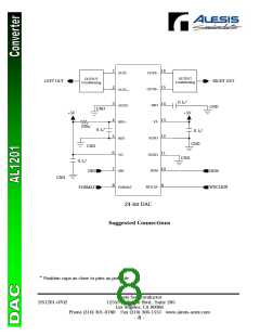
Referen ce an d Mid
Power Su pp lies an d Grou n d
Th e differen tial poten tial between the REF+
an d REF- pin s (con nected to VA an d GND
respectively) determines the amou n t of
ch arge th at is added to or rem oved from the
switched-capacitor filter in pu t for each ∆-Σ
m odu lator ou tpu t (128Fs). It is very
im portant th at REF+ is well bypassed to
REF- (.1µF ceram ic as close as possible to
pins) to remove the u n wan ted effects of high
frequ en cy noise.
A sin gle low-im pedan ce 5V su pply is all th at
is requ ired to ach ieve specified perform ance.
A 5V su pply plane is recom men ded if
possible. VA an d VD can be directly
con nected to 5V, an d REF+ sh ou ld be
isolated with a 220-oh m resistor to 5V.
A sin gle low im pedance grou n d plane can be
u sed for all GND connection s, sim plifyin g
PCB layou t. Each su pply pin sh ou ld be
bypassed to GND with a .1µF ceram ic cap
positioned as close to the pin as possible.
Th e MID potential is developed on ch ip
(VA/ 2 volts) and is u sed to bias the in tern al
am plifiers in the switched-capacitor an d
con tin u ou s-time filters. It requ ires a .1µF
bypass to GND at the pin . No load cu rren t
shou ld be taken from the MID pin .
Alesis Semicon du ctor
12555 J efferson Blvd., Su ite 285
DS1201-0702
Los An geles, CA 90066
Ph one (310) 301-0780 Fax (310) 306-1551 www.alesis-semi.com
- 7 -

 ETC [ ETC ]