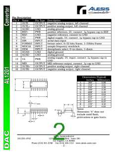
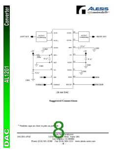
Pin Descrip t ion
Pin # Nam e
Pin Type Description
1
2
3
4
5
OUTL-
OUTL+
AGND
REF+
REF-
VD
OUTPUT n egative an alog ou tpu t, left ch an n el
OUTPUT positive an alog ou tpu t, left ch an n el
GND
PWR
GND
PWR
INPUT
an alog grou n d
positive referen ce, 5V, con n ect .1µ bypass cap to REF-
n egative referen ce, con n ect to GND
digital su pply, 5V, con n ect .1µ bypass cap to GND
serial data in pu t
6
7
DIN
8
9
10
11
12
FORMAT INPUT
form at select, 0=32 bits/ fram e, 1=24bits/ fram e
sam ple frequ en cy wordclock
deem ph asis select, 0=n o deem , 1=deem
digital grou n d
WDCLK
DEM
DGND
AGND
INPUT
INPUT
GND
GND
an alog grou n d
an alog su pply, 5V, in pu t, con n ect .1µ bypass cap to
GND
13
VA
PWR
MID
OUTR+
OUTR-
OUTPUT
14
15
16
MID referen ce ou tpu t, con n ect .1µ cap to GND
OUTPUT positive an alog ou tpu t, righ t ch an n el
OUTPUT n egative an alog ou tpu t, righ t ch an n el
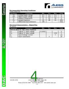
Dim en sion s (Typical)
In ch es
.389”
.154”
.236”
.100”
.008”
.025”
.050”
.017”
.011”
.170”
.033”
Millim eters
9.88
16
9
8
A
B
C
D
E
F
G
H
J
C
B
3.91
5.99
2.50
0.20
0.64
1.27
0.42
0.27
1
A
7° n om
K
L
4.32
0.83
K
Notes:
4° n om
D
Dim en sion “A” does n ot
in clu de m old flash ,
protru sion s or gate bu rrs.
H
E
J
L
G
F
Alesis Semicon du ctor
DS1201-0702
12555 J efferson Blvd., Su ite 285
Los An geles, CA 90066
Ph one (310) 301-0780 Fax (310) 306-1551 www.alesis-semi.com
- 2 -

 ETC [ ETC ]