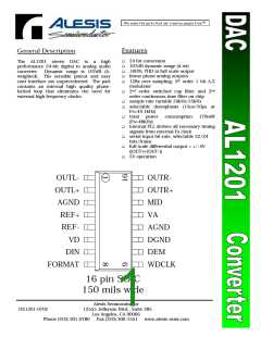
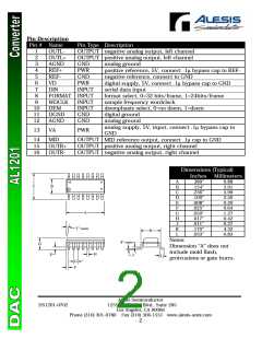
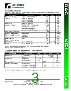
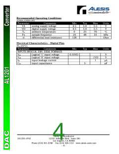
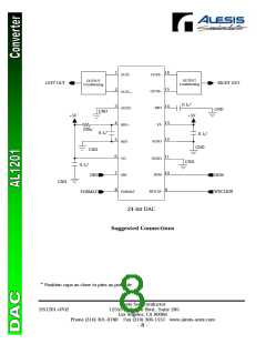
System Description
Serial In t erface an d Tim in g
In p u t Logic Levels
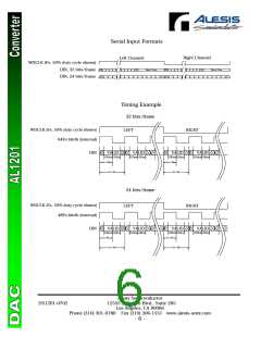
Th e AL1201 receives its 2’s com plemen t
serial data in a stan dard MSB-first form at.
Two bit-rates are allowed for. Th e 32
bits/ frame (FORMAT low) is su itable for u se
in systems where a 256Fs m aster clock is
present. Th e 24 bits/ frame (FORMAT h igh)
is con venien t when in terfacin g with systems
where a 384Fs clock is presen t.
Th e AL1201 can properly receive in pu t
logical ‘1’ voltages of .55VD. Th is m ean s the
AL1201 can interface directly with logic
sign als su pplied from 3.3V systems. No
special in terface circu itry is requ ired.
In t ern al Ph ase-Lock ed Loop (PLL)
Th e AL1201 con tains an in tern al PLL th at
locks to the rising edge of WDCLK an d
produ ces all necessary h igh frequ en cy
clocks and tim in g sign als to operate the
device. Th is h igh qu ality PLL will reject an y
h igh -frequ ency jitter on the incoming
wordclock (jitter rejection corner approx.
4kHz).
Th e in pu t sam ple period is defined between
risin g edges of wordclock (WDCLK) inpu t.
Nom in ally, this is a 50% du ty-cycle clock at
frequ en cy Fs, bu t it can be a pu lse with
Ts/ 256 < pu lse-width < Ts (255/ 256);
Ts=1/ Fs. Left ch annel data is presen ted to
the AL1201 with risin g edge of WDCLK, an d
righ t ch annel data is presen ted Ts/ 2
secon ds later (when WDCLK falls if 50%
du ty cycle).
Th e PLL allows a sim plified u ser in terface
an d elim in ates the need of ru nn in g high
frequ en cy clocks on PCB traces to the part.
Th is redu ces u n wan ted RF n oise and
cou pling problem s th at can occu r when
these clocks are requ ired as in pu t pins for a
device.
Th e serial bits are clocked in to the AL1201
in pu t registers on the falling edge of an
in tern ally generated bit clock (risin g edge
aligned with risin g edge of WDCLK) th at
ru n s at 64Fs when FORMAT is low (32
bits/ frame), or 48Fs when FORMAT is h igh
(24 bits/ fram e). Th e in pu t data shou ld be
valid +/ -100ns from the falling edge of this
in tern ally generated clock. See tim in g
diagram next page.
Alesis Semicon du ctor
12555 J efferson Blvd., Su ite 285
DS1201-0702
Los An geles, CA 90066
Ph one (310) 301-0780 Fax (310) 306-1551 www.alesis-semi.com
- 5 -

 ETC [ ETC ]