<ꢀ5ꢁꢀꢂꢃ<ꢀ.ꢁꢀꢂ
'PJCPEGFꢄ<ꢁꢀꢂꢄ/KETQRTQEGUUQT
ZiLOG
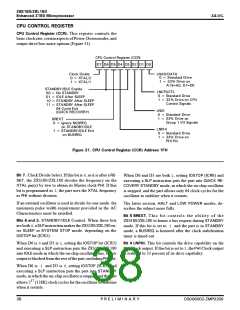
%27ꢄ%10641.ꢄ4')+56'4
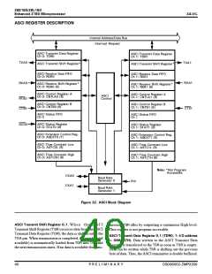
%27ꢄ%QPVTQNꢄ4GIKUVGTꢄꢌ%%4ꢍꢆꢄThis register controls the
basicclockrate, certainaspectsofPower-Downmodes, and
output drive/low-noise options (Figure 31).
%27ꢅ%QPVTQNꢅ4GIKUVGTꢅꢈ%%4ꢉ
&ꢍ
&ꢀ
&ꢂ &ꢄ
&ꢊ &ꢁ &ꢏ &ꢎ
%NQEMꢅ&KXKFG
ꢅꢀꢅꢐꢅ:6#.ꢌꢂ
ꢅꢄꢅꢐꢅ:6#.ꢌꢄ
.0#&ꢌ#
ꢀꢅꢐꢅ5VCPFCTFꢅ&TKXG
ꢄꢅꢐꢅꢍꢍꢖꢅ&TKXGꢅQP
ꢅꢅꢅꢅꢅꢅ#ꢄꢋ #ꢀꢇꢅ&ꢊ &ꢀ
56#0&$;ꢌ+&.'ꢅ'PCDNG
ꢅꢀꢀꢅꢐꢅ0Qꢅ56#0&$;
.0%27%6.
ꢅꢀꢅꢐꢅ5VCPFCTFꢅ&TKXG
ꢅꢄꢅꢐꢅꢍꢍꢖꢅ&TKXGꢅQPꢅ%27
ꢅꢅꢅꢅꢅꢅꢅꢅ%QPVTQNꢅ5KIPCNU
ꢅꢀꢄꢅꢐꢅ+&.'ꢅ#HVGTꢅ5.''2
ꢅꢄꢀꢅꢐꢅ56#0&$;ꢅ#HVGTꢅ5.''2
ꢅꢄꢄꢅꢐꢅ56#0&$;ꢅ#HVGTꢅ5.''2
ꢅꢅꢅꢅꢅꢅꢅꢅꢅꢅꢅꢁꢎꢃ%[ENGꢅ'ZKV
.0+1
ꢅꢅꢅꢅꢅꢅꢅꢅꢅꢅꢅꢈ37+%-ꢅ4'%18'4;ꢉ
ꢅꢀꢅꢐꢅ5VCPFCTFꢅ&TKXG
ꢅꢄꢅꢐꢅꢍꢍꢖꢅ&TKXGꢅQP
ꢅꢅꢅꢅꢅꢅꢅꢅ)TQWRꢅꢄꢅ+ꢌ1ꢅ5KIPCNU
$4':6
ꢅꢀꢅꢐꢅ+IPQTGꢅ$754'3
ꢅꢅꢅꢅꢅꢅꢅꢅQPꢅ56#0&$;ꢌ+&.'
ꢅꢄꢅꢐꢅ56#0&$;ꢌ+&.'ꢅ'ZKV
ꢅꢅꢅꢅꢅꢅꢅꢅꢅQPꢅ$754'3ꢅ
.02*+
ꢅꢀꢅꢐꢅ5VCPFCTFꢅ&TKXG
ꢅꢄꢅꢐꢅꢍꢍꢖꢅ&TKXGꢅQP
ꢅꢅꢅꢅꢅꢅꢅꢅ2*+ꢅ2KP
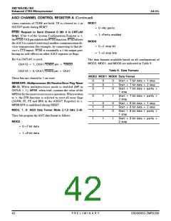
(KIWTG ꢋꢁꢆ %27ꢄ%QPVTQNꢄ4GIKUVGTꢄꢌ%%4ꢍꢄ#FFTGUUꢄꢁ(*
$KVꢄꢐꢆꢄClock Divide Select. If this bit isꢅ0, as it is after a 4'ꢃ
5'6, the Z8S180/Z8L180 divides the frequency on the
:6#. pin(s) by two to obtain its Master clock 2*+. If this
bit is programmed asꢅ1, the part uses the :6#. frequency
as 2*+ without division.
When D6 and D3 are both 1, setting +15612 (+%4ꢏ) and
executing a 5.2 instruction puts the part into 37+%-ꢅ4'ꢃ
%18'4; 56#0&$; mode, in which the on-chip oscillator
is stopped, and the part allows only 64 clock cycles for the
oscillator to stabilize when it restarts.
If an external oscillator is used in divide-by-one mode, the
minimum pulse width requirement provided in the AC
Characteristics must be satisfied.
The latter section, *#.6 and .19ꢅ219'4 modes, de-
scribes the subject more fully.
$KV ꢑ $4':6ꢆꢄThis bit controls the ability of the
Z8S180/Z8L180 to honor a bus request during 56#0&$;
mode. If this bit is set to 1 and the part is in 56#0&$;
mode, a $754'3 is honored after the clock stabilization
timer is timed out.
$KVUꢄꢈꢄCPFꢄꢋꢆꢄ56#0&$;/+&.' Control. When these bits
arebothꢅ0, a5.2 instructionmakes the Z8S180/Z8L180en-
ter 5.''2 or 5;56'/ꢅ5612 mode, depending on the
+15612 bit (ICR5).
When D6 isꢅ0and D3 isꢅ1, setting the +15612 bit (ICR5)
and executing a 5.2 instruction puts the Z8S180/Z8L180
into +&.' mode in which the on-chip oscillator runs, but its
output isblockedfromthe rest ofthe part, including2*+ out.
$KVꢄꢉꢄ.02*+ꢆꢄThis bit controls the drive capability on the
2*+ Clock output. If this bit is set to 1, the 2*+ Clock output
is reduced to 33 percent of its drive capability.
When D6 is 1 and D3 isꢅ0, setting +15612 (ICR5) and
executing a 5.2 instruction puts the part into 56#0&$;
mode, in which the on-chiposcillator is stopped and thepart
17
allows 2 (128K) clock cycles for the oscillator to stabilize
when it restarts.
ꢍꢆ
2ꢅ4ꢅ'ꢅ.ꢅ+ꢅ/ꢅ+ꢅ0ꢅ#ꢅ4ꢅ;
&5ꢀꢀꢁꢀꢀꢂꢃ</2ꢀꢂꢀꢀ

 ZILOG [ ZILOG, INC. ]