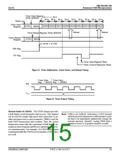
<ꢀ5ꢁꢀꢂꢃ<ꢀ.ꢁꢀꢂ
'PJCPEGFꢄ<ꢁꢀꢂꢄ/KETQRTQEGUUQT
ZiLOG
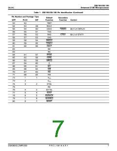
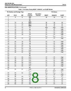
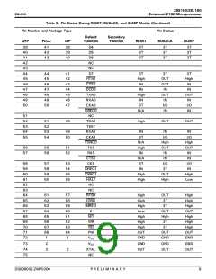
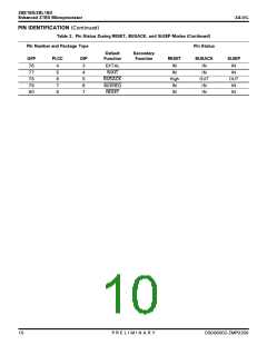
2+0ꢄ&'5%4+26+105
#ꢂ #ꢁꢏ ꢄAddress Bus (Output, 3-state). #ꢀ #ꢄꢋ form a
20-bit address bus. The Address Bus provides the address
for memory data bus exchanges (up to 1 MB) and I/O data
bus exchanges (up to 64 KB). The address bus enters a
high–impedance state during reset and external bus ac-
knowledgecycles. Addressline#ꢄꢆismultiplexedwiththe
'ꢆꢄEnable Clock (Output). This pin functions as a synchro-
nous, machine-cycle clock output during bus transactions.
':6#.ꢆꢄExternal Clock Crystal (Input). Crystal oscillator
connections. An external clock can be input to the
Z8S180/Z8L180 on this pin when a crystal is not used. This
input is Schmitt triggered.
output of PRT channel 1 (6
, selected as address output
*#.6. *#.6/5.''2 (Output, active Low). This output is
asserted after the CPU executes either the *#.6 or 5.''2
instruction and is waiting for either a nonmaskable or a
maskable interrupt before operation can resume. It is also
used with the /ꢄ and 56 signals to decode the status of the
CPU machine cycle.
on reset), and address line #ꢄꢋ is not available in DIP ver-
sions of the Z8S180.
$75#%-. Bus Acknowledge (Output, active Low).
$75#%- indicates that the requesting device, the MPU ad-
dressanddatabus, andsomecontrolsignalsentertheirhigh-
impedance state.
+06ꢂ. Maskable Interrupt Request 0 (Input, active Low).
This signal is generated by external I/O devices. The CPU
honors these requests at the end of the current instruction
cycle as long as the 0/+ and $754'3 signals are inactive.
The CPU acknowledges this interrupt request with an in-
terrupt acknowledge cycle. During this cycle, both the /ꢄ
and +143 signals become active.
$754'3ꢆꢄBus Request (Input, active Low). This input is
used by external devices (such as DMA controllers) to re-
questaccesstothesystembus. Thisrequestdemandsahigh-
er priority than 0/+ and is always recognized at the end of
the current machine cycle. This signal stops the CPU from
executing further instructions, places addresses, data buses,
and other control signals into the high-impedance state.
+06ꢁꢎꢄ+06ꢇ. Maskable Interrupt Request 1 and 2 (Inputs,
active Low). This signal is generated by external I/O de-
vices. The CPU honors these requests at the end of the cur-
rentinstructioncycleaslongasthe0/+,$754'3,and+06ꢀ
signals are inactive. The CPU acknowledges these requests
with an interrupt acknowledge cycle. Unlike the acknowl-
edgment for +06ꢀ, neither the /ꢄ or +143 signals become
active during this cycle.
%-#ꢂꢎꢄ%-#ꢁꢆꢄAsynchronous Clock 0 and 1 (bidirection-
al). When in output mode, these pins are the transmit and
receive clock outputs from the ASCI baud rate generators.
When in input mode, these pins serve as the external clock
inputs for the ASCI baud rate generators. %-#ꢀ is multi-
plexedwith&4'3ꢀ, and%-#ꢄ ismultiplexed with6'0&ꢀ.
%-5ꢆꢄSerial Clock (bidirectional). This line is the clock for
the CSI/O channel.
+143. I/O Request (Output, active Low, 3-state). +143 in-
dicates that the address bus contains a valid I/O address for
an +ꢌ1ꢅ4'#& or +ꢌ1 94+6' operation. +143 is also gener-
ated, along with /ꢄ, during the acknowledgment of the
+06ꢀ input signal to indicate that an interrupt response vec-
tor can be place onto the data bus. This signal is analogous
to the +1' signal of the Z64180.
%65ꢂ %65ꢁ. Clear to send 0 and 1 (Inputs, active Low).
These lines are modem control signals for the ASCI chan-
nels. %65ꢄ is multiplexed with 4:5.
&ꢂ &ꢐꢆꢄData Bus = (bidirectional, 3-state). &ꢀ &ꢊ con-
stitute an 8-bit bidirectional data bus, used for the transfer
of information to and from I/O and memory devices. The
data bus enters the high-impedance state during reset and
external bus acknowledge cycles.
/ꢁ. Machine Cycle 1 (Output, active Low). Together with
/4'3, /ꢄ indicates that the current cycle is the opcode-
fetch cycle of instruction execution. Together with +143,
/ꢄ indicates that the current cycle is for interrupt acknowl-
edgment. It is also used with the *#.6 and 56 signal to de-
code the status of the CPU machine cycle. This signal is
analogous to the .+4 signal of the Z64180.
&%&ꢂ. Data Carrier Detect 0 (Input, active Low); a pro-
grammable modem control signal for ASCI channel 0.
&4'3ꢂꢎꢄ&4'3ꢁ. DMA Request 0 and 1 (Input, active
Low). &4'3 is used to request a DMA transfer from one
of the on-chip DMA channels. The DMA channels monitor
these inputs to determine when an external device is ready
for a 4'#& or 94+6' operation. These inputs can be pro-
grammed to be either level or edge sensed. &4'3ꢀ is mul-
tiplexed with %-#ꢀ.
/4'3. Memory Request (Output, active Low, 3-state).
/4'3 indicates that the address bus holds a valid address
for a memory 4'#& or memory 94+6' operation. This sig-
nal is analogous to the /' signal of Z64180.
0/+. Nonmaskable Interrupt (Input, negative edge trig-
gered). 0/+ demands a higher priority than +06 and is al-
&5ꢀꢀꢁꢀꢀꢂꢃ</2ꢀꢂꢀꢀ
2ꢅ4ꢅ'ꢅ.ꢅ+ꢅ/ꢅ+ꢅ0ꢅ#ꢅ4ꢅ;
ꢄꢄ

 ZILOG [ ZILOG, INC. ]