P
R
E
L
I
M
I
N
A
R
Y
I
N
F
O
R
M
A
T
I
O
N
XpressFlow-2020 Series –
Ethernet Switch Chipset
SC220
XpressFlow Engine
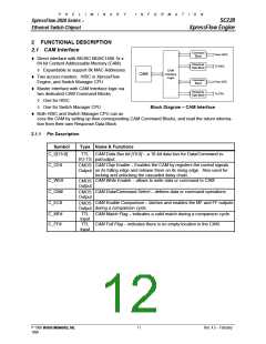
2.2 Local Memory (Control Buffer Memory) Interface
t Uses industry standard Synchronous Burst SRAM (Pipe-lined Mode)
à Supports 64k x 32, 128k x 32, or 256k x 32 chips up to maximum 2M bytes
t Provides 4 individual Byte Write Enable controls
t Supports back to back Read or Write operations
2.2.1 Pin Description
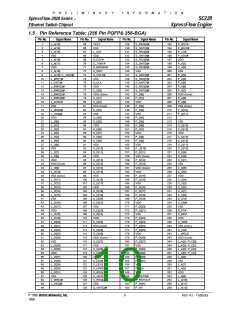
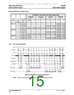
Symbol
Type Name & Functions
L_D[31:0]
TTL Local Memory Data Bus Bit [31:0] – a 32-bit synchronous data bus.
I/O-TS
L_A[18:2]
CMOS Local Memory Address Bus Bit [18:2] – Bit [17:2] of a synchronous ad-
Output
dress bus. The memory address is sampled when L_CS# is enabled
and L_ADSC# is asserted.
L_A[19] /
CMOS Local Memory Address Bus Bit [19] or Local Memory Write Chip Select
L_WE[3]#
Output
[3] – Depends on memory configuration, this pin can be used as the
Local Memory Address Bit [19] or as the Local Memory Write Chip
Select [3].
L_WE[2:0]#
L_OE[3:0]#
CMOS Local Memory Write Chip Select [2:0] – allows up to write one of the 4
Output
banks of memory.
CMOS Local Memory Read Chip Select [3:0] – allows up to read one of the 4
Output
banks of memory.
L_BWE[3:0]# CMOS Local Memory Byte Write Enable [3:0] – use to write individual bytes.
Output
L_ADSC#
L_CLK
CMOS Local Memory Controller Address Status – to load a new address.
Output
CMOS Local Memory Clock – a synchronous clock to memory devices.
Output
© 1998 Vertex Networks, Inc.
13
Rev. 4.5 – February
1999

 ZARLINK [ ZARLINK SEMICONDUCTOR INC ]