NJ88C22
1
2
(15)26
(16)27
(17)28
3
4
5
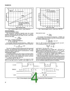
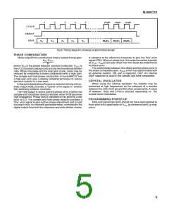
CLOCK
ENABLE
DATA
A
A
A
A
A
(M )R
(M )R
(M )R
0 0
6
5
4
3
2
2
2
1
1
Fig.6 Timing diagram showing programming details
PHASE COMPARATORS
Noise output from a synthesiser loop is related to loop gain:
KPD KVCO
is sampled at the reference frequency to give the ‘fine’ error
signal, PDA. When in phase lock, this output would be typically
at (VDD2VSS)/2 and any offset from this would be proportional
to phase error.
The relationship between this offset and the phase error is
the phase comparator gain, KPDA, which is programmable with
an external resistor, RB, and a capacitor, CAP. An internal
50pF capacitor is used in the sample and hold comparator.
N
where KPD is the phase detector constant (volts/rad), KVCO is
theVCOconstant(rad/sec/volt)andNistheoverallloopdivision
ratio. When N is large and the loop gain is low, noise may be
reduced by employing a phase comparator with a high gain.
The sample and hold phase comparator in the NJ88C22 has
a high gain and uses a double sampling technique to reduce
spurious outputs to a low level.
CRYSTAL OSCILLATOR
When using the internal oscillator, the stability may be
enhanced at high frequencies by the inclusion of a resistor
between the OSC OUT pin and the other components. A value
of between 150Ω and 270Ω is advised, depending on the
crystal series resistance.
Astandarddigitalphase/frequencydetectordrivingathree-
state output,PDB, provides a ‘coarse’ error signal to enable
fast switching between channels.
The PDB output is active until the phase error is within the
sample and hold phase detector window, when PDB becomes
high impedance. Phase-lock is indicated at this point by a low
level on LD. The sample and hold phase detector provides a
‘fine’ error signal to give further phase adjustment and to hold
theloopinlock. Aninternallygeneratedramp, controlledbythe
digital output from both the reference and main divider chains,
PROGRAMMING/POWER UP
Data and signal input pins should not have input applied to
them prior to the application of VDD, as otherwise latch-up may
occur.
5

 ZARLINK [ ZARLINK SEMICONDUCTOR INC ]