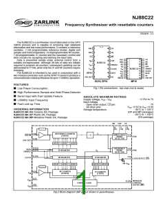
NJ88C22
PIN DESCRIPTIONS
Pin no.
Name
Description
DG,DP MP
PDA
PDB
1
1
Analog output from the sample and hold phase comparator for use as a ‘fine’ error signal. Voltage
increases as f (the output from the ‘M’ counter) phase lead increases; voltage decreases as f (the
output from the reference counter) phase lead increases. Output is linear over only a narrow phase
window, determined by gain (programmed by RB). In a type 2 loop, this pin is at (VDD2VSS)/2 when the
system is in lock.
v
r
2
2
Three-state output from the phase/frequency detector for use as a ‘coarse’ error signal.
f . f or f leading: positive pulses with respect to the bias point VBIAS
v
r
v
f , f or f leading: negative pulses with respect to the bias point VBIAS
v
r
r
f = f and phase error within PDA window: high impedance.
v
r
NC
LD
–
3
3
4
Not connected.
An open-drain lock detect output at low level when phase error is within PDA window (in lock); high
impedance at all other times.
FIN
4
5
The input to the main counters. It is normally driven from a prescaler, which may be AC-coupled or,
when a full logic swing is available, may be DC-coupled.
VSS
VDD
NC
5
6
–
6
7
8
Negative supply (ground).
Positive supply (normally 5V)
Not connected.
OSC IN/
OSC OUT
7, 8 9,10
These pins form an on-chip reference oscillator when a series resonant crystal is connected across
them. Capacitors of appropriate value are also required between each end of the crystal and ground
to provide the necessary additional phase shift. The addition of a 220Ωresistor between OSC OUT and
the crystal will improve stability. An external reference signal may, alternatively, be applied to OSC IN.
This may be a low-level signal, AC-coupled, or if a full logic swing is available it may be DC-coupled.
The program range of the reference counter is 3 to 2047 , with the total division ratio being twice the
programmed number.
NC
9
–
Not connected.
DATA
10
12
Information on this input is transferred to the internal data latches during the appropriate data read time
slot. DATA is high for a ‘1’ and low for a ‘0’. There are three data words which control the NJ88C22;
MSB is first in the order: ‘A’ (7 bits), ‘M’ (10 bits), ‘R’ (11 bits).
CLOCK
11
12
13
14
Data is clocked on the negative transition of the CLOCK waveform. If less than 28 negative clock
transitions have been received when the ENABLE line goes low (i.e., only ‘M’ and ‘A’ will have been
clockedin), thenthe‘R’counterlatchwillremainunchangedandonly‘M’and‘A’willbetransferredfrom
the input shift register to the counter latches. This will protect the ‘R’ counter from being corrupted by
any glitches on the clock line after only ‘M’ and ‘A’ have been loaded If 28 negative transitions have
been counted, then the ‘R’ counter will be loaded with the new data.
ENABLE
When ENABLE is low, the DATA and CLOCK inputs are disabled internally. As soon as ENABLE is
high, the DATA and CLOCK inputs are enabled and data may be clocked into the device. The data is
transferred from the input shift register to the counter latches on the negative transition of the ENABLE
input and both inputs to the phase detector are synchronised to each other.
CAP
MC
13
14
15
16
This pin allows an external capacitor to be connected in parallel with the internal ramp capacitor and
allows further programming of the device. (This capacitor is connected from CAP to VSS).
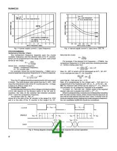
Moduluscontroloutputforcontrollinganexternaldual-modulusprescaler.MCwillbelowatthebeginning
of a count cycle and will remain low until the ‘A’ counter completes its cycle. MC then goes high and
remains high until the ‘M’ counter completes its cycle, at which point both ‘A’ and ‘M’ counters are reset.
This gives a total division ratio of MP1A, where P and P11 represent the dual-modulus prescaler
values. The program range of the ‘A’ counter is 0-127 and therefore can control prescalers with a
division ratio up to and including 4128/129. The programming range of the ‘M’ counter is 8-1023
and, for correct operation, M>A. Where every possible channel is required, the minimum total division
ratio N should be: N>P 22P, where N = MP1A.
An external sample and hold phase comparator gain programming resistor should be connected
RB
CH
15
16
17
18
between this pin and VSS
.
An external hold capacitor should be connected between this pin and VSS
.
3

 ZARLINK [ ZARLINK SEMICONDUCTOR INC ]