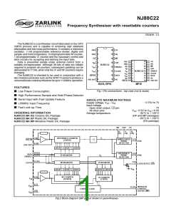
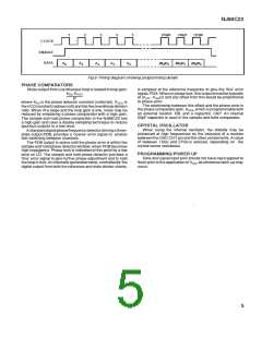
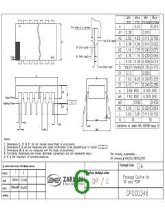
NJ88C22
ELECTRICAL CHARACTERISTICS AT VDD = 5V
Test conditions unless otherwise stated:
V
DD–VSS=5V ±0·5V. Temperature range = –40°C to +85°C
DC Characteristics
Value
Characteristic
Units
Conditions
Min. Typ. Max.
0 to 5V
square
wave
Supply current
5·5
1.5
mA
mA
f
, fFIN = 10MHz
, fFIN = 1MHz
osc
f
osc
Modulus Control Output (MC)
High level
4·6
V
V
I
I
SOURCE = 1mA
SINK = 1mA
Low level
0·4
Lock Detect Output (LD)
Low level
Open drain pull-up voltage
PDB Output
0·4
7·0
V
V
ISINK = 4mA
High level
Low level
4·6
V
V
I
SOURCE = 5mA
0·4
ISINK = 5mA
3-state leakage current
±0·1
µA
AC Characteristics
Characteristic
Value
Units
Conditions
Min. Typ.
Max.
FIN and OSC IN input level
Max. operating frequency, fFIN and f
200
20
mV RMS 10MHz AC-coupled sinewave
MHz
Input squarewave VDD to VSS,
osc
25°C.
Propagation delay, clock to modulus control MC
Programming Inputs
Clock high time, tCH
30
50
ns
See note 2
0·5
0·5
0·2
0·2
0·2
0·2
µs
µs
µs
µs
µs
µs
µs
V
Clock low time, tCL
Enable set-up time, tES
Enable hold time, tEH
Data set-up time, tDS
Data hold time, tDH
Clock rise and fall times
High level threshold
Low level threshold
All timing periods
are referenced to
the negative
transition of the
clock waveform
tCH
0·2
DD20·8
V
See note 1
See note 1
See note 1
0·8
1·0
V
V
Hysteresis
Phase Detector
Digital phase detector propagation delay
Gain programming resistor, RB
Hold capacitor, CH
Programming capacitor, CAP
Output resistance, PDA
500
5
ns
kΩ
nF
nF
kΩ
1
1
5
See note 3
NOTES
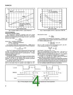
1. Data, Clock and Enable inputs are high impedance Schmitt buffers without pull-up resistors; they are therefore not TTL compatible.
2. All counters have outputs directly synchronous with their respective clock rising edges.
3. The finite output resistance of the internal voltage follower and ‘on’ resistance of the sample switch driving this pin will add a finite time constant
to the loop. An external 1nF hold capacitor will give a maximum time constant of 5µs.
4. The inputs to the device should be at logic ‘0’ when power is applied if latch-up conditions are to be avoided. This includes the signal/osc.
frequency inputs.
2

 ZARLINK [ ZARLINK SEMICONDUCTOR INC ]