MVTX2801
Data Sheet
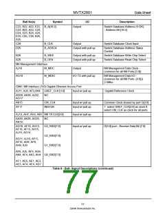
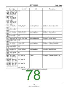
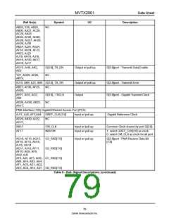
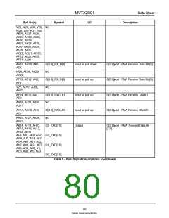
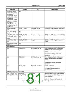
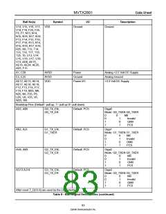
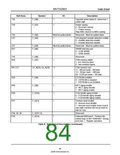
Ball No(s)
Symbol
I/O
Description
AB28, Y26, AB29,
AB30, AA27, AC28,
AC29, AA26
NC
AE26, AF28, AG30,
AG28, AG27, AH29,
AH28, AJ30
AK24, AJ24, AG24,
AF24, AH24, AF23,
AK23, AJ23
AJ19, AH19, AJ18,
AH18, AF20, AK17,
AG19, AJ17
AG13, AH8, AK2,
G[3:0]_TXD[8]
NC
Output w/ pull up
G[3:0]port - PMA Transmit Data Bit [8]
G[3:0]port - PMA Transmit Data Bit [9]
AD2
Y27, AG29, AH25,
AK19,
AJ14, AK9, AJ3, AB5 G[3:0]_TX_D[9]
Output w/ pull up
Output
AB27, AF30, AF25,
NC
AH20,
AH11, AG5, AG2,
AB4
G[3:0]_ TXCLK
NC
G[3:0]port - PMA Gigabit Transmit
Clock
AD28, AH30, AK22,
AH17,
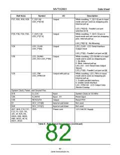
Test Facility (3)
U29
T_MODE0
T_MODE1
SCAN_EN
I/O-TS with pull up
I/O-TS with pull up
Test - Set upon Reset, and provides
NAND Tree test output during test
mode
Use external Pull up for normal
operation
Test - Set upon Reset, and provides
NAND Tree test output during test
mode.
U28
A3
Use external Pull up for normal
operation
Enable test mode
Input with pull down
Output
For normal operation leave it
unconnected
LED Interface (serial and parallel)
R28, T26, R27, T27, T_D[7:0]/
While resetting, T_D[7,0] are in input
mode and are used as strapping pins.
Internal pull up
U27, T28, T29, T30
LED_PD[7:0]
LED_PD - Parallel Led data [7:0]
Table 8 - Ball- Signal Descriptions (continued)
81
Zarlink Semiconductor Inc.

 ZARLINK [ ZARLINK SEMICONDUCTOR INC ]