MT8809
Data Sheet
28
27
26
25
24
23
22
21
20
19
18
17
16
15
1
2
3
4
5
6
7
8
AY2
STROBE
CS
AY1
AY0
AX2
AX1
AX0
X1
X3
X5
X7
VDD
Y0
DATA
VSS
X0
•
VSS
AX1
AX0
X1
5
25
24
23
22
21
20
19
6
X0
X2
X4
X6
7
X2
X4
X6
8
X3
9
X5
X7
VDD
9
RESET
Y7
10
11
RESET
Y7
10
11
12
13
14
Y6
Y5
Y4
Y1
Y2
Y3
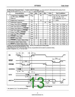
28 PIN PLCC
28 PIN PLASTIC DIP
Figure 2 - Pin Connections
Description
Pin Description
Pin #
Name
1
2
AY2
AY2 Address Line (Input).
STROBE STROBE (Input): enables function selected by address and data. Address must be stable
before STROBE goes low and DATA must be stable on the rising edge of STROBE. Active
Low.
3
4
CS
Chip Select (Input): this is used to select the device. Active Low.
DATA DATA (Input): a logic high input will turn on the selected switch and a logic low will turn off
the selected switch. Active High.
5
VSS
Ground Reference.
6-9
X0, X2, X0, X2, X4 and X6 Analog (Inputs/Outputs): these are connected to the X0, X2, X4 and
X4, X6 X6 rows of the switch array.
10
RESET Master RESET (Input): this is used to turn off all switches regardless of the condition of
CS. A 100 kΩ internal pull-up resistor is also provided. This can be used in conjunction
with a 0.1 µF capacitor (connected to the RESET pin) to perform power-on reset of the
device. Active Low.
11-18
Y7 - Y0 Y7 - Y0 Analog (Inputs/Outputs): these are connected to the Y0 - Y7 columns of the
switch array.
19
VDD
Positive Power Supply.
20-23
X7, X5, X7, X5, X3 and X1 Analog (Inputs/Outputs): these are connected to the X7, X5, X3 and
X3, X1 X1 rows of the switch array.
24-26
AX0-AX2 AX0 - AX2 Address Lines (Inputs).
27, 28 AY0, AY1 AY0 and AY1 Address Lines (Inputs).
2
Zarlink Semiconductor Inc.

 ZARLINK [ ZARLINK SEMICONDUCTOR INC ]