MT8809
ISO-CMOS
8x8 Analog Switch Array
Data Sheet
September 2005
Features
•
•
•
•
•
•
•
•
•
•
Internal control latches and address decoder
Ordering Information
Short setup and hold times
MT8809AE
28 Pin PDIP
28 Pin PLCC
28 Pin PLCC
28 Pin PLCC* Tubes
28 Pin PLCC* Tape & Reel
28 Pin PDIP* Tubes
Tubes
MT8809AP
Tubes
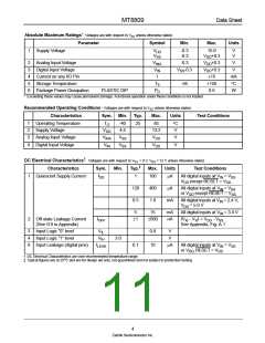
Wide operating voltage: 4.5 V to 13.2 V
12 Vpp analog signal capability
MT8809APR
MT8809AP1
MT8809APR1
MT8809AE1
Tape & Reel
R
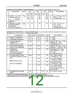
ON 65 Ω max. @ VDD = 12 V, 25°C
* Pb Free Matte Tin
∆RON ≤ 10 Ω @ VDD = 12 V, 25C
-40°C to +85°C
Full CMOS switch for low distortion
Minimum feedthrough and crosstalk
Low power consumption ISO-CMOS technology
Internal pull-up resistor for RESET pin
Description
The Zarlink MT8809 is fabricated in Zarlink’s ISO-
CMOS technology providing low power dissipation and
high reliability. The device contains a 8 x 8 array of
crosspoint switches along with a 6 to 64 line decoder
and latch circuits. Any one of the 64 switches can be
addressed by selecting the appropriate six address
bits. The selected switch can be turned on or off by
applying a logical one or zero to the DATA input. Chip
Select (CS) allows the crosspoint array to be cascaded
for matrix expansion.
Applications
•
•
•
•
•
•
Key systems
PBX systems
Mobile radio
Test equipment/instrumentation
Analog/digital multiplexers
Audio/Video switching
STROBE
DATA RESET
VDD
VSS
CS
1
1
AX0
AX1
AX2
AY0
AY1
AY2
8 x 8
Switch
Array
6 to 64
Decoder
Xi I/O
(i=0-7)
Latches
64
64
• • • • • • • • • • • • • • • • • • •
Yi I/O (i=0-7)
Figure 1 - Functional Block Diagram
1
Zarlink Semiconductor Inc.
Zarlink, ZL and the Zarlink Semiconductor logo are trademarks of Zarlink Semiconductor Inc.
Copyright 1988 - 2005, Zarlink Semiconductor Inc. All Rights Reserved.

 ZARLINK [ ZARLINK SEMICONDUCTOR INC ]