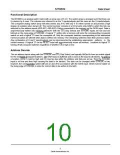
MT8809
Data Sheet
AC Electrical Characteristics† - Control and I/O Timings- VDC is the external DC offset applied at the analog I/O pins.
Voltages are with respect to VDD = 5 V, VDC = 0 V, VSS = -7 V, unless otherwise stated.
Characteristics
Sym.
Min. Typ.‡ Max.
Units
Test Conditions
1
Control Input crosstalk to switch
(for CS, DATA, STROBE,
Address)
CXtalk
30
mVpp VIN=3V+VDC squarewave;
RIN=1 k, RL=1 k.
See Appendix, Fig. A.6
2
3
4
5
6
7
8
9
Digital Input Capacitance
CDI
FO
10
pF
MHz
ns
f = 1 MHz
Switching Frequency
20
Setup Time DATA to STROBE
Hold Time DATA to STROBE
Setup Time Address to STROBE
Hold Time Address to STROBE
Setup Time CS to STROBE
Hold Time CS to STROBE
tDS
tDH
tAS
tAH
tCSS
tCSH
tSPW
tRPW
tS
10
10
10
10
10
10
20
40
RL= 1 k, CL= 50 pF ¿ Å
RL= 1 k, CL= 50 pF Å¿
RL= 1 k, CL= 50 pF Å¿
RL= 1 k, CL= 50 pF Å¿
RL= 1 k, CL= 50 pF Å¿
RL= 1 k, CL= 50 pF ¿Å
RL= 1 k, CL= 50 pF ¿Å
RL= 1 k, CL= 50 pF Å¿
RL= 1 k, CL=50 pF Å¿
RL= 1 k, CL= 50 pF Å¿
RL= 1 k, CL= 50 pF ¿Å
ns
ns
ns
ns
ns
10 STROBE Pulse Width
ns
11 RESET Pulse Width
ns
12 STROBE to Switch Status Delay
13 DATA to Switch Status Delay
14 RESET to Switch Status Delay
40
50
35
100
100
100
ns
tD
ns
tR
ns
† Timing is over recommended temperature range. See Fig. 3 for control and I/O timing details.
Digital Input rise time (tr) and fall time (tf) = 5 ns.
‡ Typical figures are at 25C and are for design aid only; not guaranteed and not subject to production testing.
Å¿Refer to Appendix, Fig. A.7 for test circuit.
tCSS
50%
tCSH
50%
CS
tRPW
RESET
tSPW
50%
50%
50%
50%
50%
STROBE
50%
tAS
50%
tAH
ADDRESS
DATA
50%
tDS
50%
tDH
ON
SWITCH*OFF
tR
tR
tS
tD
Figure 3 - Control Memory Timing Diagram
* See Appendix, Fig. A.7 for switching waveform
6
Zarlink Semiconductor Inc.

 ZARLINK [ ZARLINK SEMICONDUCTOR INC ]