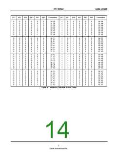
MT8809
Data Sheet
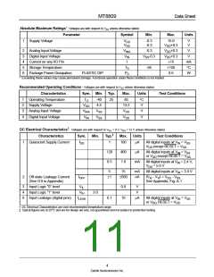
Absolute Maximum Ratings*- Voltages are with respect to VSS unless otherwise stated.
Parameter
Symbol
Min.
Max.
Units
1
Supply Voltage
VDD
VSS
-0.3
-0.3
15.0
DD+0.3
V
V
V
2
3
4
5
6
Analog Input Voltage
Digital Input Voltage
VINA
VIN
I
-0.3
VDD+0.3
VDD+0.3
±15
V
VSS-0.3
V
Current on any I/O Pin
Storage Temperature
mA
°C
W
TS
PD
-65
+150
Package Power Dissipation
PLASTIC DIP
0.6
* Exceeding these values may cause permanent damage. Functional operation under these conditions is not implied.
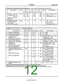
Recommended Operating Conditions - Voltages are with respect to VSS unless otherwise stated.
Characteristics
Sym. Min.
Typ.
Max.
Units
Test Conditions
1
2
3
Operating Temperature
Supply Voltage
TO
-40
4.5
25
85
°C
V
VDD
VINA
13.2
VDD
Analog Input Voltage
VSS
V
4
Digital Input Voltage
VIN
VSS
VDD
V
DC Electrical Characteristics†- Voltages are with respect to VSS = 0 V, VDD = 12 V unless otherwise stated.
Characteristics
Sym.
Min.
Typ.‡
Max.
Units
Test Conditions
1
2
Quiescent Supply Current
IDD
1
100
µA
All digital inputs at VIN = VSS
VDD except RESET = VDD.
120
0.5
400
1.6
µA
All digital inputs at VIN = VSS
or VDD except RESET = VSS.
mA
All digital inputs at VIN = 2.4 V,
VDD = 5.0 V
5
15
mA
nA
All digital inputs at VIN = 3.4 V
Off-state Leakage Current
(See G.9 in Appendix)
IOFF
±1
±500
IVXi - VYjI = VDD - VSS
See Appendix, Fig. A.1
3
4
6
Input Logic “0” level
VIL
VIH
0.8
10
V
V
Input Logic “1” level
3.0
Input Leakage (digital pins)
ILEAK
0.1
µA
All digital inputs at VIN = VSS
or VDD; RESET = VDD
† DC Electrical Characteristics are over recommended temperature range.
‡ Typical figures are at 25°C and are for design aid only; not guaranteed and not subject to production testing.
4
Zarlink Semiconductor Inc.

 ZARLINK [ ZARLINK SEMICONDUCTOR INC ]