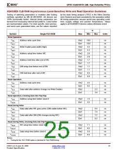
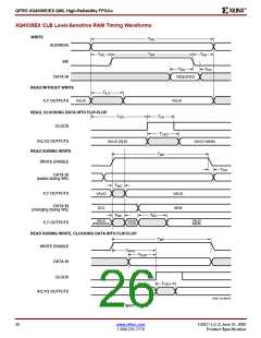
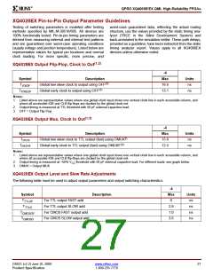
R
QPRO XQ4000E/EX QML High-Reliability FPGAs
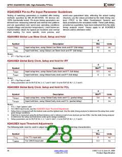
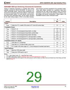
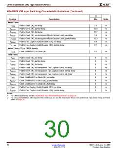
XQ4028EX IOB Input Switching Characteristic Guidelines
Testing of switching parameters is modeled after testing
methods specified by MIL-M-38510/605. All devices are
100% functionally tested. Internal timing parameters are
derived from measuring internal test patterns. Listed below
are representative values. For more specific, more precise,
and worst-case guaranteed data, use the values reported
by the static timing analyzer (TRCE in the Xilinx Develop-
ment System) and back-annotated to the simulation netlist.
These path delays, provided as a guideline, have been
extracted from the static timing analyzer report. All timing
parameters assume worst-case operating conditions (sup-
ply voltage and junction temperature). Values apply to all
XQ4000EX devices unless otherwise noted.
-4
Symbol
Clocks
Description
Min
Units
T
Delay from FCL enable (OK) active to IFF clock (IK) active edge
3.2
ns
OKIK
Propagation Delays
T
Pad to I1, I2
2.2
3.8
ns
ns
ns
ns
ns
ns
PID
T
Pad to I1, I2 via transparent input latch, no delay
Pad to I1, I2 via transparent input latch, partial delay
Pad to I1, I2 via transparent input latch, full delay
Pad to I1, I2 via transparent FCL and input latch, no delay
Pad to I1, I2 via transparent FCL and input latch, partial delay
PLI
T
T
13.3
18.2
5.3
PPLI
PDLI
T
PFLI
T
13.6
PPFLI
Propagation Delays (TTL Inputs)
T
Clock (IK) to I1, I2 (flip-flop)
3.0
3.2
6.2
ns
ns
ns
IKRI
T
Clock (IK) to I1, I2 (latch enable, active Low)
IKLI
T
FCL enable (OK) active edge to I1, I2 (via transparent standard input latch)
OKLI
Global Set/Reset
T
Minimum GSR pulse width
13.0
22.8
ns
ns
MRW
T
Delay from GSR input to any Q
RRI
Notes:
1. FCL = Fast Capture Latch, IFF = Input Flip-Flop or Latch
2. For CMOS input levels, see the "XQ4028EX Input Threshold Adjustments" on page 28.
3. For setup and hold times with respect to the clock input pin, see the Global Low Skew Clock and Global Early Clock Setup and Hold
tables on page 28.
DS021 (v2.2) June 25, 2000
www.xilinx.com
29
Product Specification
1-800-255-7778

 XILINX [ XILINX, INC ]