Virtex-6 FPGA Data Sheet: DC and Switching Characteristics
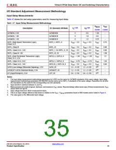
I/O Standard Adjustment Measurement Methodology
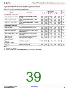
Input Delay Measurements
Table 47 shows the test setup parameters used for measuring input delay.
Table 47: Input Delay Measurement Methodology
VMEAS
VREF
(1)(2)
(1)(2)
Description
I/O Standard Attribute
VL
VH
(1)(4)(5)
(1)(3)(5)
LVCMOS, 2.5V
LVCMOS, 1.8V
LVCMOS, 1.5V
LVCMOS25
0
0
0
2.5
1.8
1.25
0.9
–
–
LVCMOS18
LVCMOS15
1.5
0.75
VREF
–
HSTL (High-Speed Transceiver Logic),
Class I & II
HSTL_I, HSTL_II
V
REF – 0.5
VREF + 0.5
0.75
HSTL, Class III
HSTL_III
VREF – 0.5
REF – 0.5
VREF – 0.5
VREF + 0.5
VREF + 0.5
VREF + 0.5
VREF + 1.00
VREF
VREF
VREF
VREF
0.90
0.90
1.08
1.5
HSTL, Class I & II, 1.8V
HSTL, Class III 1.8V
HSTL_I_18, HSTL_II_18
HSTL_III_18
V
SSTL (Stub Terminated Transceiver Logic),
Class I & II, 3.3V
SSTL3_I, SSTL3_II
VREF – 1.00
SSTL, Class I & II, 2.5V
SSTL2_I, SSTL2_II
SSTL18_I, SSTL18_II
LVDS_25
V
REF – 0.75
VREF + 0.75
VREF + 0.5
1.2 + 0.125
1.2 + 0.125
0.6 + 0.125
VREF
VREF
0(6)
1.25
0.90
–
SSTL, Class I & II, 1.8V
VREF – 0.5
LVDS (Low-Voltage Differential Signaling), 2.5V
LVDSEXT (LVDS Extended Mode), 2.5V
HT (HyperTransport), 2.5V
1.2 – 0.125
1.2 – 0.125
0.6 – 0.125
LVDSEXT_25
LDT_25
0(6)
–
0(6)
–
Notes:
1. The input delay measurement methodology parameters for LVDCI are the same for LVCMOS standards of the same voltage. Input delay
measurement methodology parameters for HSLVDCI are the same as for HSTL_II standards of the same voltage. Parameters for all other
DCI standards are the same for the corresponding non-DCI standards.
2. Input waveform switches between V and V .
L
H
3. Measurements are made at typical, minimum, and maximum V
values listed are typical.
values. Reported delays reflect worst case of these measurements. V
REF
REF
4. Input voltage level from which measurement starts.
5. This is an input voltage reference that bears no relation to the V
6. The value given is the differential input voltage.
/ V
parameters found in IBIS models and/or noted in Figure 6.
REF
MEAS
DS152 (v3.6) March 18, 2014
www.xilinx.com
Product Specification
35

 XILINX [ XILINX, INC ]