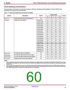
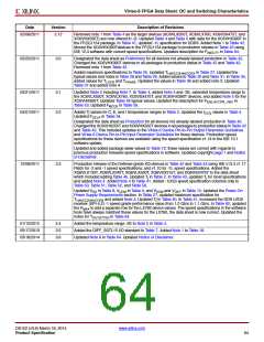
Virtex-6 FPGA Data Sheet: DC and Switching Characteristics
Clock Switching Characteristics
The parameters in this section provide the necessary values for calculating timing budgets for Virtex-6 FPGA clock
transmitter and receiver data-valid windows.
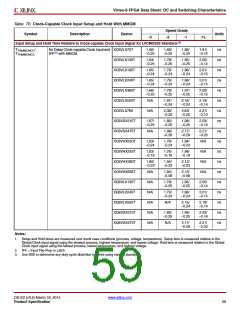
Table 71: Duty Cycle Distortion and Clock-Tree Skew
Speed Grade
Symbol
Description
Device
Units
-3
-2
-1
-1L
0.12
0.17
0.28
0.30
0.30
0.31
0.54
0.56
0.30
0.42
N/A
TDCD_CLK
Global Clock Tree Duty Cycle Distortion(1)
Global Clock Tree Skew(2)
All
0.12
0.15
0.25
0.26
0.26
0.28
N/A
N/A
0.27
N/A
0.25
0.35
0.45
N/A
N/A
N/A
N/A
N/A
N/A
0.08
0.03
0.10
0.15
0.12
0.16
0.26
0.27
0.27
0.29
0.50
0.51
0.28
0.39
0.26
0.37
0.47
0.46
0.26
0.27
N/A
0.12
0.18
0.29
0.31
0.31
0.31
0.54
0.56
0.32
0.44
0.29
0.41
0.52
0.51
0.29
0.31
0.54
0.32
0.44
0.08
0.03
0.23
0.15
ns
ns
ns
ns
ns
ns
ns
ns
ns
ns
ns
ns
ns
ns
ns
ns
ns
ns
ns
ns
ns
ns
ns
TCKSKEW
XC6VLX75T
XC6VLX130T
XC6VLX195T
XC6VLX240T
XC6VLX365T
XC6VLX550T
XC6VLX760
XC6VSX315T
XC6VSX475T
XC6VHX250T
XC6VHX255T
XC6VHX380T
XC6VHX565T
XQ6VLX130T
XQ6VLX240T
XQ6VLX550T
XQ6VSX315T
XQ6VSX475T
All
N/A
N/A
N/A
0.28
0.30
0.54
0.30
0.42
0.08
0.02
0.12
0.15
0.28
N/A
TDCD_BUFIO
TBUFIOSKEW
TBUFIOSKEW2
TDCD_BUFR
I/O clock tree duty cycle distortion
0.08
0.03
0.12
0.15
I/O clock tree skew across one clock region
I/O clock tree skew across three clock regions
Regional clock tree duty cycle distortion
All
All
All
Notes:
1. These parameters represent the worst-case duty cycle distortion observable at the pins of the device using LVDS output buffers. For cases
where other I/O standards are used, IBIS can be used to calculate any additional duty cycle distortion that might be caused by asymmetrical
rise/fall times.
2. The T
value represents the worst-case clock-tree skew observable between sequential I/O elements. Significantly less clock-tree
CKSKEW
skew exists for I/O registers that are close to each other and fed by the same or adjacent clock-tree branches. Use the Xilinx FPGA_Editor
and Timing Analyzer tools to evaluate clock skew specific to your application.
DS152 (v3.6) March 18, 2014
www.xilinx.com
Product Specification
60

 XILINX [ XILINX, INC ]