Spartan-3E FPGA Family: Pinout Descriptions
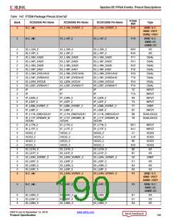
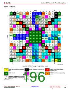
The XC3S250E FPGA in the FT256 package has 18
unconnected balls, labeled with an “N.C.” type. These pins
are also indicated with the black diamond () symbol in
Figure 85.
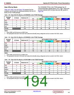
User I/Os by Bank
Table 143, Table 144, and Table 145 indicate how the
available user-I/O pins are distributed between the four I/O
banks on the FT256 package.
Table 143: User I/Os Per Bank on XC3S250E in the FT256 Package
All Possible I/O Pins by Type
Package
Edge
I/O Bank
Maximum I/O
(2)
I/O
20
10
8
INPUT
DUAL
1
VREF(1)
CLK
Top
0
1
2
3
44
42
10
7
5
4
8
Right
21
24
0
0(2)
0(2)
8
Bottom
Left
44
9
3
42
24
62
7
3
TOTAL
172
33
46
15
16
Notes:
1. Some VREF and CLK pins are on INPUT pins.
2. The eight global clock pins in this bank have optional functionality during configuration and are counted in the DUAL column.
Table 144: User I/Os Per Bank on XC3S500E in the FT256 Package
All Possible I/O Pins by Type
Package
I/O Bank
Maximum I/O
Edge
(2)
I/O
22
15
11
28
76
INPUT
DUAL
VREF(1)
CLK
8
Top
0
1
2
3
46
48
10
7
1
5
5
Right
21
24
0
0(2)
0(2)
8
Bottom
Left
48
9
4
48
7
5
TOTAL
190
33
46
19
16
Notes:
1. Some VREF and CLK pins are on INPUT pins.
2. The eight global clock pins in this bank have optional functionality during configuration and are counted in the DUAL column.
.
Table 145: User I/Os Per Bank on XC3S1200E in the FT256 Package
All Possible I/O Pins by Type
Package
Edge
I/O Bank
Maximum I/O
(2)
I/O
24
14
13
27
78
INPUT
DUAL
1
VREF(1)
CLK
8
Top
0
1
2
3
46
48
8
8
5
5
Right
21
24
0
0(2)
0(2)
8
Bottom
Left
48
7
4
48
8
5
TOTAL
190
31
46
19
16
Notes:
1. Some VREF and CLK pins are on INPUT pins.
2. The eight global clock pins in this bank have optional functionality during configuration and are counted in the DUAL column.
DS312 (v4.2) December 14, 2018
www.xilinx.com
Product Specification
194

 XILINX [ XILINX, INC ]