R
Platform Flash XL High-Density Configuration and Storage Device
Pinout and Signal Descriptions
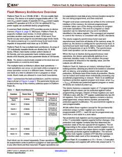
See Figure 5 and Table 2 for a logic diagram and brief overview of the signals connected to this device.
X-Ref Target - Figure 5
Table 2: Signal Names
VDD
VDDQ
VPP
Signal Name
Function
Direction
A22-A0
Address Inputs
Inputs
23
16
Data Input/Outputs,
Command Inputs
DQ15-DQ0
I/O
DQ15–DQ0
A22–A0
E
Chip Enable
Output Enable
Write Enable
Reset
Input
Input
Input
Input
Input
Input
Input
I/O
W
E
G
W
READY_WAIT
RP
G
Platform
Flash XL
WP
Write Protect
Clock
RP
WP
L
K
L
Latch Enable
Ready/Wait
Supply Voltage
READY_WAIT
VDD
–
Supply Voltage for
Input/Output Buffers
K
VDDQ
–
–
Optional(1) Supply
Voltage for Fast
Program and Erase
VPP
VSS
VSSQ
DS617_05_053008
VSS
Ground
–
–
Figure 5: Logic Diagram
GroundInput/output
Supply
VSSQ
Not Connected
Internally
NC
–
Notes:
1. Typically, V is tied to the V
supply on a board. See the V
PP
PP
DDQ
Program Supply Voltage section for alternate options.
deselected, the outputs are high impedance, and the power
consumption is reduced to the standby level.
Address Inputs (A22-A0)
The Address inputs select the words in the memory array to
access during Bus Read operations. During Bus Write
operations they control the commands sent to the
Command Interface of the Program/Erase Controller.
Output Enable (G)
The Output Enable input controls data outputs during the
Bus Read operation of the memory. Before the start of the
first address latching sequence (FALS), the Output Enable
input must be held Low before the clock starts toggling.
Data Inputs/Outputs (DQ15-DQ0)
The Data I/O output the data stored at the selected address
during a Bus Read operation or input a command or the
data to be programmed during a Bus Write operation.
Write Enable (W)
The Write Enable input controls the Bus Write operation of
the memory’s Command Interface. The data and address
inputs are latched on the rising edge of Chip Enable or
Write Enable, whichever occurs first.
Chip Enable (E)
The Chip Enable input activates the memory control logic,
input buffers, decoders and sense amplifiers. When Chip
Enable is at V and Reset is at V , the device is in active
IL
IH
mode. When Chip Enable is at V , the memory is
IH
DS617 (v3.0.1) January 07, 2010
www.xilinx.com
Product Specification
5

 XILINX [ XILINX, INC ]