R
Platform Flash XL High-Density Configuration and Storage Device
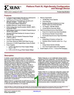
X-Ref Target - Figure 1
FPGA
Platform Flash XL
Configuration
Synchronization
Handshake
READY_WAIT
Clock up to 50 MHz(1)
Wide (16-bit) Datapath
Up to 800 Mb/s
FPGA Design
(.bit) File
DS617_01_102709
Notes:
1. System considerations can lower the configuration clock frequency below the maximum clock frequency for the device. To determine the
maximum configuration clock frequency, check the minimum clock period (T
) for the chosen I/O voltage range (V
), the clock High-
KHKH
DDQ
to-output valid time (T
), and the FPGA SelectMAP setup time.
KHQV
Figure 1: Platform Flash XL Delivers Reliable, High-Performance FPGA Configuration
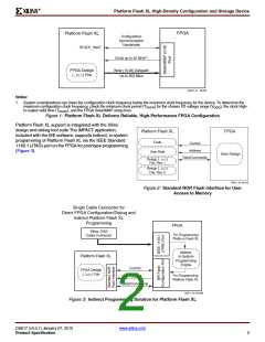
X-Ref Target - Figure 2
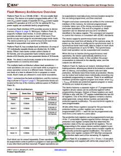
Platform Flash XL support is integrated with the Xilinx
design and debug tool suite.The iMPACT application,
included with the ISE software, supports indirect, in-system
programming of Platform Flash XL via the IEEE Standard
1149.1 (JTAG) port on the FPGA for prototype programming
(Figure 3).
Platform Flash XL
FPGA
Code
Control
Address
User Data
User Design
Data/Commands
Design (.bit)
File, Rev. 1
Design (.bit)
File, Rev. 0
DS617_02_081209
Figure 2: Standard NOR Flash Interface for User
Access to Memory
X-Ref Target - Figure 3
Single Cable Connector for
Direct FPGA Configuration/Debug and
Indirect Platform Flash XL
Programming
FPGA
Xilinx JTAG
Cable Connector
For Programming
Platform Flash XL
Indirect,
In-System
Programming
Engine
Platform Flash XL
Control
FPGA Design
(.bit) File
For Programming
Platform Flash XL
Address
Data/Commands
DS617_03_081209
Figure 3: Indirect Programming Solution for Platform Flash XL
DS617 (v3.0.1) January 07, 2010
www.xilinx.com
Product Specification
2

 XILINX [ XILINX, INC ]