R
Virtex-II Platform FPGAs: Introduction and Overview
SelectRAM, and block SelectRAM memory resources can
be read back. This capability is useful for real-time debug-
ging.
Boundary Scan
Boundary scan instructions and associated data registers
support a standard methodology for accessing and config-
uring Virtex-II devices that complies with IEEE standards
1149.1 — 1993 and 1532. A system mode and a test mode
are implemented. In system mode, a Virtex-II device per-
forms its intended mission even while executing non-test
boundary-scan instructions. In test mode, boundary-scan
test instructions control the I/O pins for testing purposes.
The Virtex-II Test Access Port (TAP) supports BYPASS,
PRELOAD, SAMPLE, IDCODE, and USERCODE non-test
instructions. The EXTEST, INTEST, and HIGHZ test instruc-
tions are also supported.
The Integrated Logic Analyzer (ILA) core and software pro-
vides a complete solution for accessing and verifying
Virtex-II devices.
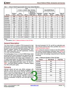
Virtex-II Device/Package Combinations
and Maximum I/O
Wire-bond and flip-chip packages are available. Table 4 and
Table 5 show the maximum possible number of user I/Os in
wire-bond and flip-chip packages, respectively. Table 6
shows the number of available user I/Os for all device/pack-
age combinations.
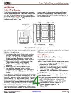
Configuration
Virtex-II devices are configured by loading data into internal
configuration memory, using the following five modes:
•
CS denotes wire-bond chip-scale ball grid array (BGA)
(0.80 mm pitch).
•
CSG denotes Pb-free wire-bond chip-scale ball grid
array (BGA) (0.80 mm pitch).
FG denotes wire-bond fine-pitch BGA (1.00 mm pitch).
FGG denotes Pb-free wire-bond fine-pitch BGA (1.00
mm pitch).
BG denotes standard BGA (1.27 mm pitch).
BGG denotes Pb-free standard BGA (1.27 mm pitch).
FF denotes flip-chip fine-pitch BGA (1.00 mm pitch).
BF denotes flip-chip BGA (1.27 mm pitch).
•
•
•
•
•
Slave-serial mode
Master-serial mode
Slave SelectMAP mode
Master SelectMAP mode
Boundary-Scan mode (IEEE 1532)
•
•
•
•
•
•
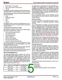
A Data Encryption Standard (DES) decryptor is available
on-chip to secure the bitstreams. One or two triple-DES key
sets can be used to optionally encrypt the configuration
information.
The number of I/Os per package include all user I/Os except
the 15 control pins (CCLK, DONE, M0, M1, M2, PROG_B,
PWRDWN_B, TCK, TDI, TDO, TMS, HSWAP_EN, DXN,
DXP, and RSVD) and VBATT.
Readback and Integrated Logic Analyzer
Configuration data stored in Virtex-II configuration memory
can be read back for verification. Along with the configura-
tion data, the contents of all flip-flops/latches, distributed
Table 4: Wire-Bond Packages Information
CS144/
CSG144
FG256/
FGG256
FG456/
FGG456
FG676/
FGG676
BG575/
BGG575
BG728/
BGG728
(1)
Package
Pitch (mm)
0.80
12 x 12
92
1.00
17 x 17
172
1.00
23 x 23
324
1.00
27 x 27
484
1.27
31 x 31
408
1.27
35 x 35
516
Size (mm)
I/Os
Notes:
1. Wire-bond packages include FGGnnn Pb-free versions. See Virtex-II Ordering Examples (Module 1).
Table 5: Flip-Chip Packages Information
Package
Pitch (mm)
FF896
1.00
FF1152
1.00
FF1517
1.00
BF957
1.27
Size (mm)
I/Os
31 x 31
624
35 x 35
824
40 x 40
1,108
40 x 40
684
DS031-1 (v3.5) November 5, 2007
Product Specification
www.xilinx.com
Module 1 of 4
5

 XILINX [ XILINX, INC ]