R
Virtex-II Platform FPGAs: Introduction and Overview
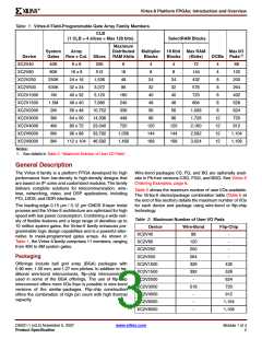
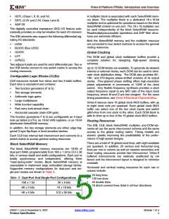
Table 1: Virtex-II Field-Programmable Gate Array Family Members
CLB
(1 CLB = 4 slices = Max 128 bits)
SelectRAM Blocks
Maximum
System
Gates Row x Col. Slices
Array
Distributed
RAM Kbits
Multiplier 18 Kbit Max RAM
Max I/O
DCMs Pads
(1)
Device
XC2V40
Blocks
4
Blocks
4
(Kbits)
72
40K
80K
250K
500K
1M
8 x 8
16 x 8
256
8
16
4
4
88
120
200
264
432
528
624
720
912
1,104
1,108
XC2V80
512
8
8
144
XC2V250
XC2V500
XC2V1000
XC2V1500
XC2V2000
XC2V3000
XC2V4000
XC2V6000
XC2V8000
Notes:
24 x 16
32 x 24
40 x 32
48 x 40
56 x 48
64 x 56
80 x 72
96 x 88
112 x 104
1,536
3,072
5,120
7,680
10,752
14,336
23,040
33,792
46,592
48
24
24
432
8
96
32
32
576
8
160
240
336
448
720
1,056
1,456
40
40
720
8
1.5M
2M
48
48
864
8
56
56
1,008
1,728
2,160
2,592
3,024
8
3M
96
96
12
12
12
12
4M
120
144
168
120
144
168
6M
8M
1. See details in Table 2, “Maximum Number of User I/O Pads”.
General Description
The Virtex-II family is a platform FPGA developed for high
performance from low-density to high-density designs that
are based on IP cores and customized modules. The family
delivers complete solutions for telecommunication, wire-
less, networking, video, and DSP applications, including
PCI, LVDS, and DDR interfaces.
Wire-bond packages CS, FG, and BG are optionally avail-
abe in Pb-free versions CSG, FGG, and BGG. See Virtex-II
Ordering Examples, page 6.
Table 2 shows the maximum number of user I/Os available.
The Virtex-II device/package combination table (Table 6 at
the end of this section) details the maximum number of I/Os
for each device and package using wire-bond or flip-chip
technology.
The leading-edge 0.15 µm / 0.12 µm CMOS 8-layer metal
process and the Virtex-II architecture are optimized for high
speed with low power consumption. Combining a wide vari-
ety of flexible features and a large range of densities up to
10 million system gates, the Virtex-II family enhances pro-
grammable logic design capabilities and is a powerful alter-
native to mask-programmed gates arrays. As shown in
Table 1, the Virtex-II family comprises 11 members, ranging
from 40K to 8M system gates.
Table 2: Maximum Number of User I/O Pads
Device
XC2V40
Wire-Bond
Flip-Chip
88
120
200
264
328
392
-
-
-
XC2V80
XC2V250
XC2V500
XC2V1000
XC2V1500
XC2V2000
XC2V3000
XC2V4000
XC2V6000
XC2V8000
-
Packaging
-
Offerings include ball grid array (BGA) packages with
0.80 mm, 1.00 mm, and 1.27 mm pitches. In addition to tra-
ditional wire-bond interconnects, flip-chip interconnect is
used in some of the BGA offerings. The use of flip-chip
interconnect offers more I/Os than is possible in wire-bond
versions of the similar packages. Flip-chip construction
offers the combination of high pin count with high thermal
capacity.
432
528
624
720
912
1,104
1,108
516
-
-
-
DS031-1 (v3.5) November 5, 2007
Product Specification
www.xilinx.com
Module 1 of 4
2

 XILINX [ XILINX, INC ]