X28LC512/X28LC513
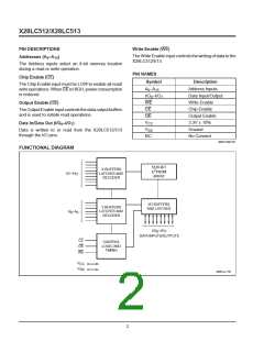
PIN DESCRIPTIONS
Write Enable (WE)
The Write Enable input controls the writing of data to the
X28LC512/513.
Addresses (A –A )
0
15
The Address inputs select an 8-bit memory location
during a read or write operation.
PIN NAMES
Chip Enable (CE)
Symbol
Description
Address Inputs
Data Input/Output
Write Enable
Chip Enable
Output Enable
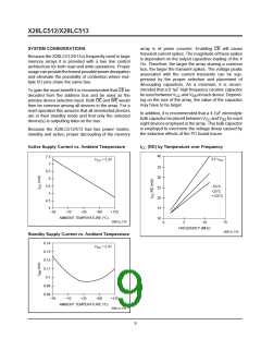
3.3V ± 10%
The Chip Enable input must be LOW to enable all read/
writeoperations.WhenCEisHIGH,powerconsumption
is reduced.
A –A
0
15
I/O –I/O
0
7
WE
CE
OE
Output Enable (OE)
TheOutputEnableinputcontrolsthedataoutputbuffers
and is used to initiate read operations.
V
CC
Data In/Data Out (I/O –I/O )
0
7
V
Ground
Data is written to or read from the X28LC512/513
through the I/O pins.
SS
NC
No Connect
3005 PGM T01
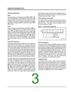
FUNCTIONAL DIAGRAM
512K-BIT
E PROM
ARRAY
X BUFFERS
LATCHES AND
DECODER
2
A –A
7
15
I/O BUFFERS
AND LATCHES
Y BUFFERS
LATCHES AND
DECODER
A –A
0
6
I/O –I/O
0
7
DATA INPUTS/OUTPUTS
CE
OE
CONTROL
LOGIC AND
TIMING
WE
V
CC
V
SS
3005 ILL F01
2

 XICOR [ XICOR INC. ]