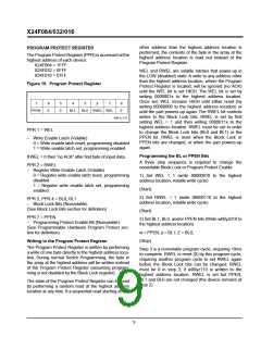
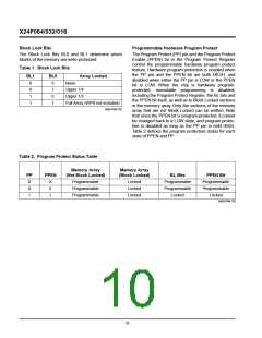
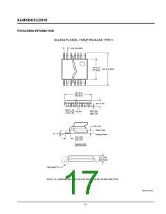
X24F064/032/016
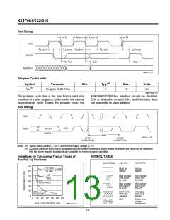
Bus Timing
t
t
t
R
t
HIGH
LOW
F
SCL
t
t
t
t
t
SU:STO
SU:STA
HD:STA
HD:DAT
SU:DAT
SDA IN
t
t
t
AA
DH
BUF
SDA OUT
6686 ILL F17
Program Cycle Limits
(5)
Symbol
Parameter
Min.
Typ.
Max.
Units
(6)
tPR
Program Cycle Time
5
10
ms
6686 FRM T11.1
The program cycle time is the time from a valid stop
condition of a write sequence to the end of the internal
erase/program cycle. During the program cycle, the
X24F064/032/016 bus interface circuits are disabled,
SDA is allowed to remain HIGH, and the device does
not respond to its slave address.
Bus Timing
SCL
ACK
SDA
8th BIT
WORD n
t
WR
6686 ILL F18
STOP
CONDITION
START
CONDITION
Notes: (5) Typical values are for T = 25°C and nominal supply voltage (2.7V).
A
(6) t
is the minimum cycle time to be allowed from the system perspective unless polling techniques are used. It is the maximum
WR
time the device requires to automatically complete the internal program operation.
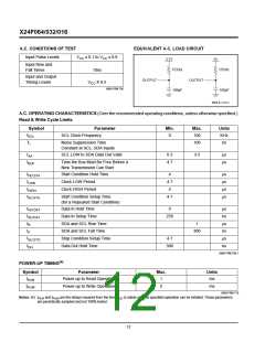
Guidelines for Calculating Typical Values of
Bus Pull-Up Resistors
SYMBOL TABLE
WAVEFORM
INPUTS
OUTPUTS
120
V
CC MAX
Must be
steady
Will be
steady
R
=
=1.2KΩ
MIN
I
100
80
OL MIN
t
R
May change
from LOW
to HIGH
Will change
from LOW
to HIGH
R
=
MAX
C
BUS
MAX.
60
40
20
0
RESISTANCE
May change
from HIGH
to LOW
Will change
from HIGH
to LOW
MIN.
Don’t Care:
Changes
Allowed
Changing:
State Not
Known
RESISTANCE
20 40 60 80
120
100
0
N/A
Center Line
is High
Impedance
BUS CAPACITANCE (pF)
6686 ILL F19.1
13

 XICOR [ XICOR INC. ]