X24C01
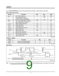
WRITE CYCLE LIMITS
(5)
Symbol
Parameter
Write Cycle Time
Min.
Typ.
Max.
Units
(6)
t
5
10
ms
WR
3837 PGM T08
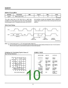
The write cycle time is the time from a valid stop
condition of a write sequence to the end of the internal
erase/programcycle.Duringthewritecycle,theX24C01
bus interface circuits are disabled, SDA is allowed to
remainhigh, andthedevicedoesnotrespondtoitsword
address.
Write Cycle Timing
SCL
ACK
SDA
8th BIT
WORD n
t
WR
STOP
CONDITION
START
CONDITION
X24C01
ADDRESS
3837 FHD F05
Notes: (5) Typical values are for T = 25°C and nominal supply voltage (5V).
A
(6) t
is the minimum cycle time to be allowed from the system perspective unless polling techniques are used. It is the maximum
WR
time the device requires to automatically complete the internal write operation.
Guidelines for Calculating Typical Values of
Bus Pull-Up Resistors
SYMBOL TABLE
WAVEFORM
INPUTS
OUTPUTS
120
Must be
steady
Will be
steady
V
CC MAX
R
=
=2.6KΩ
MIN
I
100
80
OL MIN
t
May change
from Low to
High
Will change
from Low to
High
R
R
=
MAX
C
BUS
MAX.
60
40
20
0
RESISTANCE
May change
from High to
Low
Will change
from High to
Low
MIN.
Don’t Care:
Changes
Allowed
Changing:
State Not
Known
RESISTANCE
20 40 60 80
120
100
0
Center Line
is High
Impedance
N/A
BUS CAPACITANCE (pF)
3837 FHD F15
10

 XICOR [ XICOR INC. ]