WM8904
Pre-Production
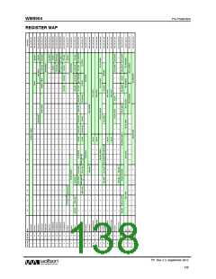
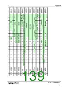
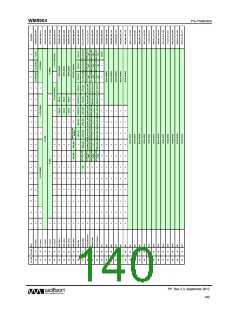
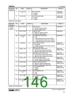
REGISTER BITS BY ADDRESS
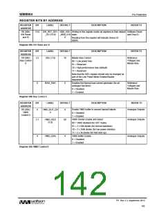
REGISTER
ADDRESS
BIT
LABEL
DEFAULT
DESCRIPTION
REFER TO
Writing to this register resets all registers to their default Software Reset
R0 (00h)
SW Reset
and ID
15:0
SW_RST_DEV 1000_1001
state.
and Chip ID
_ID1 [15:0]
_0000_010
0
Reading from this register will indicate Device ID
8904h.
Register 00h SW Reset and ID
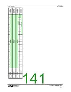
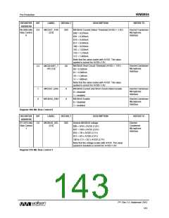
REGISTER
ADDRESS
BIT
LABEL
DEFAULT
DESCRIPTION
REFER TO
Master Bias Control
00 = Low power bias
01 = Reserved
Reference
Voltages and
Master Bias
R4 (04h)
Bias Control
0
3:2
ISEL [1:0]
10
10 = High performance bias (default)
11 = Reserved
Note that the ISEL register should only be changed as
part of the Low Power Mode Enable/Disable
sequences.
Enables the Normal bias current generator (for all
analogue functions)
Reference
Voltages and
Master Bias
0
BIAS_ENA
0
0 = Disabled
1 = Enabled
Register 04h Bias Control 0
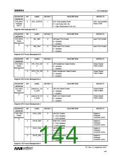
REGISTER
ADDRESS
BIT
LABEL
DEFAULT
DESCRIPTION
REFER TO
Enable VMID buffer to unused Inputs/Outputs
0 = Disabled
Analogue Outputs
R5 (05h)
VMID
Control 0
6
VMID_BUF_EN
A
0
1 = Enabled
VMID Divider Enable and Select
00 = VMID disabled (for OFF mode)
01 = 2 x 50k divider (for normal operation)
10 = 2 x 250k divider (for low power standby)
11 = 2 x 5k divider (for fast start-up)
VMID Buffer Enable
Analogue Outputs
Analogue Outputs
2:1
VMID_RES
[1:0]
00
0
VMID_ENA
0
0 = Disabled
1 = Enabled
Register 05h VMID Control 0
PP, Rev 3.3, September 2012
142
w

 WOLFSON [ WOLFSON MICROELECTRONICS PLC ]