Production Data
WM8352
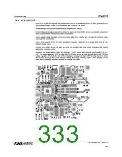
29.6 PCB LAYOUT
Poor PCB layout will degrade the performance and be a contributory factor in EMI, ground bounce
and resistive voltage losses. Poor regulation and instability can result.
Simple design rules can be implemented to negate these effects:
External input and output capacitors should be placed as close to the device as possible using short
wide traces between the external power components.
Route output voltage feedback on an inner plane away from inductor and LX nodes to minimise noise
and magnetic interference.
Use a local ground island for each individual converter connected at a single point onto a fully
flooded ground plane.
Current loop areas should be kept as small as possible with loop areas changing little during
alternating switching cycles.
Studying the layout below shows, for example, DCDC1 layout with external components C16, L3,
C17. The input capacitor, C16, is close into the IC and shares a small ground island with C17 the
output capacitor. The inductor, L3, is then situated in close proximity to C17 to keep loop area small
and current flowing in the same direction during alternating switching cycles. Note also the use of
short wide traces with all power tracking on a single (top) layer.
PD, February 2011, Rev 4.4
333
w

 WOLFSON [ WOLFSON MICROELECTRONICS PLC ]