WM8352
Production Data
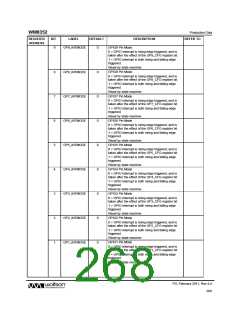
REFER TO
REGISTER
ADDRESS
BIT
LABEL
DEFAULT
DESCRIPTION
Input:
0 = Active low
1 = Active high
Output:
0 = CMOS
1 = Open drain
Reset by state machine. Default held in metal mask.
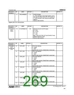
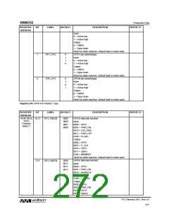
1
GP1_CFG
0
1
1
0
GPIO1 pin polarity/type:
Input:
0 = Active low
1 = Active high
Output:
0 = CMOS
1 = Open drain
Reset by state machine. Default held in metal mask.
0
GP0_CFG
0
1
0
1
GPIO0 pin polarity/type:
Input:
0 = Active low
1 = Active high
Output:
0 = CMOS
1 = Open drain
Reset by state machine. Default held in metal mask.
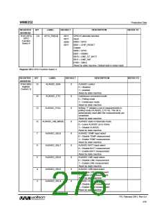
Register 87h GPIO Pin Polarity / Type
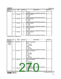
REGISTER
ADDRESS
BIT
LABEL
DEFAULT
DESCRIPTION
REFER TO
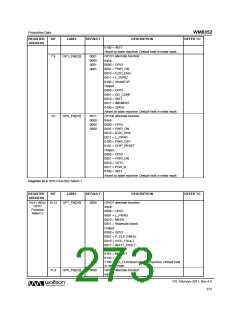
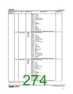
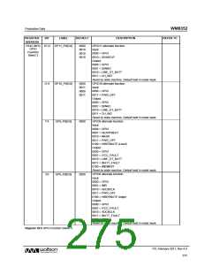
R140 (8Ch) 15:12
GPIO
Function
GP3_FN[3:0]
0000
0000
0001
0000
GPIO3 alternate function:
Input:
0000 = GPIO
Select 1
0001 = PWR_ON
0010 = LDO_ENA
0011 = PWR_OFF
0100 = FLASH
Output:
0000 = GPIO
0001 = P_CLK
0010 = VRTC
0011 = 32kHz
0100 = /MEMRST
Reset by state machine. Default held in metal mask.
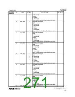
GPIO2 alternate function:
Input:
11:8
GP2_FN[3:0]
0000
0011
0011
0011
0000 = GPIO
0001 = PWR_ON
0010 = /WAKEUP
0011 = 32KHZ
0100 = L_PWR3
Output:
0000 = GPIO
0001 = PWR_ON
0010 = VRTC
0011 = 32KHZ
PD, February 2011, Rev 4.4
272
w

 WOLFSON [ WOLFSON MICROELECTRONICS PLC ]