Production Data
WM8352
REGISTER
ADDRESS
BIT
LABEL
DEFAULT
DESCRIPTION
REFER TO
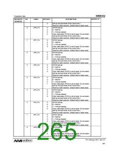
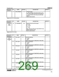
0
GP0_INTMODE
0
GPIO0 Pin Mode
0 = GPIO interrupt is rising edge triggered, and is
taken after the effect of the GP0_CFG register bit.
1 = GPIO interrupt is both rising and falling edge
triggered.
Reset by state machine.
Register 83h GPIO Interrupt Mode
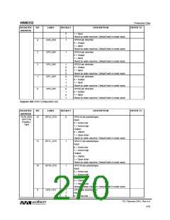
REGISTER
ADDRESS
BIT
LABEL
DEFAULT
DESCRIPTION
REFER TO
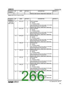
R133 (85h)
GPIO
Control
7:6
GP_DBTIME[1:0]
00
Debounce time for all GPIO inputs
00 = 64us
01 = 0.5ms
10 = 1ms
11 = 4ms
Note: PWR_ON, PWR_OFF and /WAKEUP have
additional debounce times.
Reset by state machine.
Register 85h GPIO Control
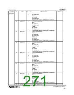
REGISTER
ADDRESS
BIT
LABEL
DEFAULT
DESCRIPTION
REFER TO
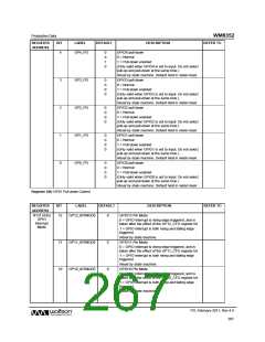
R134 (86h)
GPIO
12
GP12_DIR
0
GPIO12 pin direction
0 = Output
Configuratio
n (i/o)
1 = Input
Reset by state machine. Default held in metal mask.
11
10
9
GP11_DIR
GP10_DIR
GP9_DIR
GP8_DIR
GP7_DIR
GP6_DIR
GP5_DIR
1
GPIO11 pin direction
0 = Output
1 = Input
Reset by state machine. Default held in metal mask.
1
0
0
0
1
1
0
1
1
GPIO10 pin direction
0 = Output
1 = Input
Reset by state machine. Default held in metal mask.
GPIO9 pin direction
0 = Output
1 = Input
Reset by state machine. Default held in metal mask.
8
GPIO8 pin direction
0 = Output
1 = Input
Reset by state machine. Default held in metal mask.
7
1
1
GPIO7 pin direction
0 = Output
1 = Input
Reset by state machine. Default held in metal mask.
6
GPIO6 pin direction
0 = Output
1 = Input
Reset by state machine. Default held in metal mask.
GPIO5 pin direction
5
1
1
0 = Output
PD, February 2011, Rev 4.4
269
w

 WOLFSON [ WOLFSON MICROELECTRONICS PLC ]