Production Data
WM8326
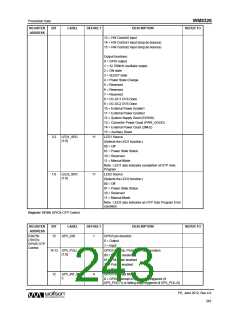
REGISTER
ADDRESS
BIT
LABEL
DEFAULT
DESCRIPTION
13 = HW Control2 input
REFER TO
14 = HW Control1 input (long de-bounce)
15 = HW Control2 input (long de-bounce)
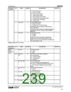
Output functions:
0 = GPIO output
1 = 32.768kHz oscillator output
2 = ON state
3 = SLEEP state
4 = Power State Change
5 = Reserved
6 = Reserved
7 = Reserved
8 = DC-DC1 DVS Done
9 = DC-DC2 DVS Done
10 = External Power Enable1
11 = External Power Enable2
12 = System Supply Good (SYSOK)
13 = Converter Power Good (PWR_GOOD)
14 = External Power Clock (2MHz)
15 = Auxiliary Reset
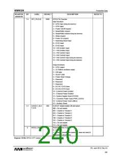
LED1 Source
LED1_SRC
[1:0]
3:2
11
(Selects the LED1 function.)
00 = Off
01 = Power State Status
10 = Reserved
11 = Manual Mode
Note - LED1 also indicates completion of OTP Auto
Program
LED2_SRC
[1:0]
LED2 Source
1:0
11
(Selects the LED2 function.)
00 = Off
01 = Power State Status
10 = Reserved
11 = Manual Mode
Note - LED2 also indicates an OTP Auto Program Error
condition
Register 781Dh GPIO4 OTP Control
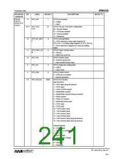
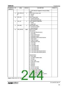
REGISTER
ADDRESS
BIT
LABEL
GP5_DIR
DEFAULT
DESCRIPTION
REFER TO
R30750
(781Eh)
GPIO5 pin direction
0 = Output
15
1
GPIO5 OTP
Control
1 = Input
GP5_PULL
[1:0]
GPIO5 Pull-Up / Pull-Down configuration
00 = No pull resistor
01 = Pull-down enabled
10 = Pull-up enabled
11 = Reserved
14:13
01
GP5_INT_MOD
E
GPIO5 Interrupt Mode
12
0
0 = GPIO interrupt is rising edge triggered (if
GP5_POL=1) or falling edge triggered (if GP5_POL=0)
PD, June 2012, Rev 4.0
243
w

 WOLFSON [ WOLFSON MICROELECTRONICS PLC ]